- Home
- Publications
- Journal of the Electron Devices Society
- Editor-in-Chief and Editors
Editor-in-Chief and Editors
J-EDS is constantly looking for world-class and motivated Editors to join our editorial board to edit and approve manuscripts for inclusion in the J-EDS.
If you are interested in serving as a J-EDS editor, please contact the current Editor-In-Chief Man Wong for more information.
If you wish to be added to the list of potential reviewers in the EDS database, please contact the EDS headquarters. Kindly provide your full name, email address, and area of expertise.
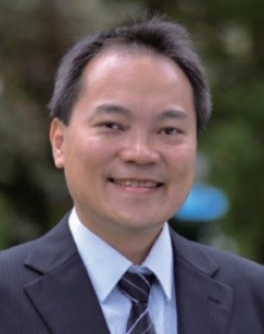
J-EDS Editor-in-Chief
Man Wong - EIC
Hong Kong
Research Areas: Fabrication technology and physical MEMS devices
Professional Memberships: IEEE, SID
Biography: Man Wong was born in Beijing, China. From 1979 to 1984, he studied at the Massachusetts Institute of Technology, USA, where he obtained his BS and MS degrees in Electrical Engineering. From 1985 to 1988, he was at the Center for Integrated Systems at Stanford University, USA, where he worked on tungsten-gate MOS technology and obtained his PhD degree, also in Electrical Engineering. From 1988 to 1992, he was with the Semiconductor Process and Design Center of Texas Instruments, USA and worked on the modeling and development of integrated-circuit metallization systems and dry/vapor surface-conditioning processes. He is currently with the Department of Electronic and Computer Engineering at the Hong Kong University of Science and Technology, Hong Kong. His research interests include micro-fabrication technology, device structure and material; physics and technology of thin-film transistor; organic light-emitting diode display technology; modeling and implementation of integrated micro-systems; and thin-film solar cell device and process technology. He is a member of Tau Beta Pi, Eta Kappa Nu and Sigma Xi. He was appointed an Honorary Guest Professor of Nankai University, Tianjin, China, in 2003 and a Visiting Professor of Soochow University, Suzhou, China, in 2011.
J-EDS Editors
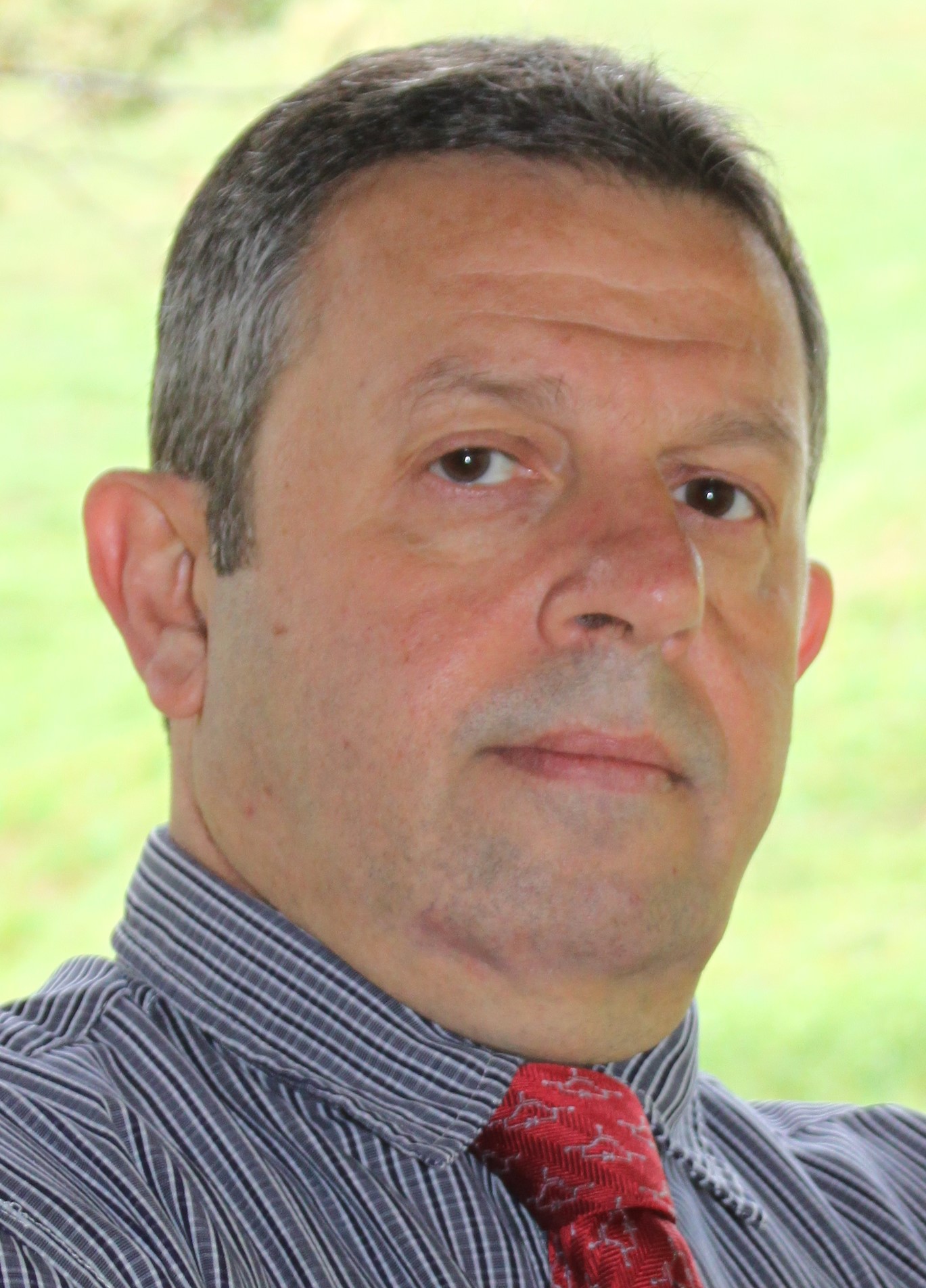
Constantin Bulucea - Distinguished Member of the Technical Staff
USA
Constantin Bulucea (S'69–M'70–SM'88–F'04- LF'13) was born in Râmnicu Vâlcea, Romania. In 1969, he got a one-year government scholarship at the University of California, Berkeley, where he received a M.S. degree in Electrical Engineering. In 1974, he received his Doctor degree in Electronics from the Polytechnic Institute of Bucharest with a thesis on hot-carrier injection in silicon. His original results were communicated at IEDM and published in the old (W. Crawford Dunlap’s) Solid-State Electronics. In Romania, he created the Annual Conference on Semiconductors, now an international IEEE event. His best known contribution from that period is the explanation of Grove’s breakdown voltage collapse in silicon gate-controlled devices as a breakdown-location switching phenomenon, as proven by 2-D computer calculations and measurements. Among his “firsts” from the same time is the direct proof, by DC recordings (rather than by capacitive inferences) of nA-range hot-carrier currents through silicon dioxide.
In 1886, Dr. Bulucea defected to the US, where he first developed a device/process architecture for rugged trench power DMOS transistors, while working for Siliconix (1987-1989). His inventive design became a world standard in the following years. Later on, at National Semiconductor (NS), he was a member of the Fairchild Research Center, then joined the company’s process development group. There, he enjoyed the last years of Silicon Valley's "Happy Scaling" as the architect of several CMOS processes for high-performance analog and mixed-signal applications (2000-2010). In 2011, he became a Distinguished Member of the Technical Staff of Texas Instruments (TI), as a result of TI's acquisition of NSC. Throughout his tenure at NS and TI, he received three Patent of the Year awards, in recognition of the use of his inventions in high-volume manufacturing. He has published over 50 technical articles in major journals and has 70 issued US patents. In 2001, he was elected an Honorary Member of the Romanian Academy and in 2004 became an IEEE Fellow "for contributions to transistor engineering in the area of power electronics".
Dr. Bulucea has been a member of the Technical Committees of the Bipolar Circuits and Technology Meeting (BCTM) and of the VLSI Technology Symposium. Between 2004 and 2012 he was the editor of IEEE Electron Device Letters (EDL) for analog and mixed-signals technology. His IEEE responsibilities include membership in the IEEE/EDS Fellow Evaluation Committee (2018, 2019) and the IEEE/EDS Publications Committee (current).
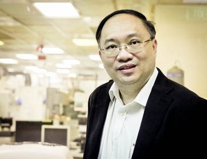
Kangguo Cheng - Silicon Technology
Kangguo Cheng (Fellow, IEEE) received the bachelor’s degree and the master’s degree from Tsinghua University, China, in 1995 and 1997, respectively, and the Ph.D. degree from University of Illinois at Urbana-Champaign in 2001.
His career started at IBM Semiconductor Research and Development Center (SRDC), Fishkill, NY. He worked on the development of vertical transistor DRAM, and later development of embedded DRAM (eDRAM) for high performance applications. In 2008 he moved to IBM Research at Albany, NY, working on a variety of technologies, including fully depleted SOI (FDSOI), FinFET, gate-all-around (GAA), emerging memories, artificial intelligence (AI) hardware, field-programmable gate array (FPGA), and emulation and prototyping of system-on-chip (SoC) chips. He is one of world’s top prolific inventors with over 2500 issued US patents. He coauthored overall more than 100 papers, two book chapters, and gave multiple invited talks.
Dr. Cheng served as a Chair of Semiconductor Invention Review Board of IBM. He also served on multiple international conference committees in semiconductor technology. He has received Invention Achievement Awards (IAA) and Outstanding Technology Achievement Award (OTAA) from IBM. He is a recipient of 2021 IEEE Paul Rappaport Award. He is a Master Inventor of IBM, a member of IBM Academy of Technology (AoT), and a Fellow of the IEEE Electron Devices Society.
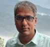
Kaustubh Joshi - Reliability of Devices and Circuits
Kaustubh Joshi (Member, IEEE) received his PhD from IIT Bombay, India in 2014.
From 2014 to 2020 he worked at TSMC, Taiwan as a Principal Engineer at Technology Quality and Reliability Division. Since 2020 he is working as Quality and Reliability R&D Engineer at Intel Corporation, Hillsboro. His primary focus has been on understanding reliability degradation in highly scaled transistors and building models and methodologies to understand device reliability. He has co-authored over 25 papers with nearly 1000 citations in the field of device reliability physics. His research interest includes physics, characterization, modelling of reliability of scaled transistors and high power III-V devices. Dr. Joshi has also served in various JEDEC committees and chair/vice-chair at IRPS conference.
Ming-Dou Ker - ESD, System Reliability
Electronics Engineering
Sriram Krishnamoorthy - Optoelectronics Device
USA
M.Jagadesh Kumar - Senior Member
Professor of Electrical Engineering
Lecture Topics: 1) Nanowire electronics: the future of CMOS technology 2) Green Transistors for energy efficient integrated circuits 3) Can Bipolar Transistors be made without doping? 4) Tunnel field effect transistors: Design and Optimization 5) Trench power MOSFETs: Design and Optimization 6) Perspectives on the evolution of semiconductor manufacturing: Enabling the impossible
Dr. Kumar is currently the NXP (Philips) Chair Professor established at IIT Delhi by Philips Semiconductors, Netherlands (now NXP Semiconductors India Pvt Ltd). He was the Co-ordinator of VLSI Design, Tools and Technology interdisciplinary program. He is a Chief Investigator of the Nano-scale Research Facility (NRF) at IIT Delhi. Dr. Kumar received the 2013 Award for Excellence in Teaching (in large class category) from IIT Delhi. He works in the area of Nanoelectronic Devices, Device modeling and simulation, IC Technology and Power semiconductor devices. He has published extensively in the above areas with four book chapters and more than 160 publications in refereed journals and conferences. He is on the Editorial Board of Scientific Reviews, an online and open access primary research publication from the publishers of Nature. He is an Editor of IEEE Transactions on Electron Devices and the Editor-in-Chief of IETE Technical Review. Dr. Kumar is a Fellow of Indian National Academy of Engineering, The National Academy of Sciences, India, and The Institution of Electronics and Telecommunication Engineers, India. He has been awarded the 29th IETE Ram Lal Wadhwa Gold Medal for distinguished contribution in the field of Semiconductor device design and modeling. He has received the first ever ISA-VSI TechnoMentor Award given by the India Semiconductor Association to recognize a distinguished Indian academician and researcher for playing a significant role as a mentor and researcher. He is a recipient of 2008 IBM Faculty award in recognition of professional achievements. He has delivered a number of invited lectures in conferences and workshops in India and abroad to large audiences on topics related to Nanoelectronics. For more details on Dr. Kumar, you can visit http://web.iitd.ac.in/~mamidala
Pei-Wen Li - Silicon Technology, Emerging Technologies, Device and Circuit Simulation"
Electronics Engineering, Hsinchu Taiwan
Pei-Wen Li (Senior Member, IEEE) received her Ph.D. degree in electrical engineering from Columbia University in New York City in 1994.
Since 2015, she is a Professor in the Institute of Electronics at National Chiao Tung University (NCTU) (as National Yang Ming Chiao Tung University (NYCU) in 2021). Prior to joining NCTU in 2015, she was a Distinguished Professor, Chair of Electrical Engineering Department, and Director of Nano Science and Technology at National Central University. She was a Research Visiting Scholar at Caltech in 2011-2012. She worked with Vanguard International Semiconductor Corporation on DRAM technology integration in 1995-1996. Her research themes focus on experimental germanium nanostructures and devices, encompassing quantum-dot single-electron transistors, photodetectors, light emitters, and thermoelectric devices, making use of self-assembly nanostructures in silicon integration technology. She has published more than 300 technical journal and conference papers and holds 8 patents.
Dr. Li is an IEEE Distinguished Lecturer and has served on the VLSI Technology and Education committees of IEEE Electron Devices Society. She has been an editorial board member of Applied Physics A, Springer since 2020. She is a senior member of the IEEE Electron Device Society and serves on various IEEE conference committees (Silicon Nanoelectronics Workshop (SNW) and Electron Devices Technology and Manufacturing (EDTM) Conference).
Sheng-Shian Li
Institute of NanoEngineering and MicroSystems, Taiwan
Sheng-Shian Li (Senior Member, IEEE) received the B.S. and M.S. degrees in mechanical engineering from National Taiwan University, Taipei, Taiwan, in 1996 and 1998, respectively, and the M.S. and Ph.D. degrees in electrical engineering and computer science from the University of Michigan, Ann Arbor, MI, USA, in 2004 and 2007, respectively.
In 2008, he joined the Institute of NanoEngineering and MicroSystems (iNEMS), National Tsing Hua University (NTHU), Hsinchu, Taiwan, where he is currently a NTHU Distinguished Professor. His research interests include MEMS/NEMS, integrated resonators and sensors, RF MEMS, CMOS-MEMS technology, frontend communication architectures, and integrated circuit design and technology. He was a recipient of the Teaching Excellence Award 2019 and Young Faculty Research Award 2013 from the National Tsing Hua University. He also received the Ta-Yu Wu Memorial Award from the National Science Council (NSC) of Taiwan in 2013 and the Outstanding Research Award from the Ministry of Science and Technology (MOST) of Taiwan in 2020. Together with his students, he received the Best Paper Awards at the 2011 IEEE International Frequency Control Symposium, the 2012 IEEE Sensors Conference, and the 2017/2023 Transducers Conference. He has served as the TPC/ETPC of the IEEE International Frequency Control Symposium, the IEEE Sensors Conference, the Transducers Conference, the IEEE MEMS Conference, and IEEE IEDM. Dr. Li also serves as the Associate Editors of the IEEE Sensors Letters, the IEEE Sensors Journal, and the IEEE JMEMS. He is appointed as General Co-Chair for 2025 IEEE MEMS Conference.
Geok Ing Ng - Compound Devices and RF Applications
Munaf Rahimo - Power Devices
Munaf T. A Rahimo (Senior Member, IEEE) received his B.Sc. in Electrical Engineering in 1990 from Baghdad University, Iraq. He then studied at Staffordshire University, UK, where he completed his M.Sc. in Electrical and Electronic Engineering with distinction in 1993 and his Ph.D. in 1996 with the thesis entitled "Switching Characteristics of Fast Power Diodes in IGBT Circuits".
In 1996, he joined GEC Plessey Semiconductors, UK developing fast diodes for IGBT and GTO applications. He joined Semelab in 1999 as a Senior Engineer developing discrete fast diodes and was involved in the early development of Silicon Carbide Schottky diodes. In 2000, he joined ABB Semiconductors, Switzerland as a Senior Research and Development Engineer. At ABB, he was involved in the development of a wide range of power devices such as IGBTs, Diodes, IGCTs, Thyrsitors, Silicon Carbide Devices and Power Modules. He pioneered many device concepts including for example the High-Voltage Planar and Enhanced-Planar IGBT, the Bimode IGBT (BIGT) and the HighPower-Technology IGCT. Due to his many contributions, he scaled ABB`s technical career path to become Chief Engineer in 2005 and Senior Principal Engineer in 2009. He was then awarded the prestigious Corporate Executive Engineer title in 2012 due to his key device innovations and contributions to HVDC systems. In 2018, he started his consulting business MTAL GmbH and founded a power device start-up mqSemi AG where he currently acts as general manager for both companies in Switzerland.
He has over 150 peer-reviewed publications and more than 100 patent applications with more than 50 granted U.S. patents. He is a member of the IEEE societies EDS, PELS and IAS.
Sunny Sadana
Department of Electrical Engineering
Sunny Sadana graduated with Master’s in Electrical Engineering from IIT Bombay in year 2011. He joined GlobalFoundries Singapore as Process Integration Engineer in 2011 where he worked on Technology development for Embedded Flash Memory at advanced nodes for 4.5 years, after that he joined IIT Bombay as Executive Scientist in Electrical Engineering department working on development of OTP memory development and its application as Random Number generator. Since 2019, he has been working as Senior Engineer in Micron Technology where he was working on reliability and technology qualification of advanced 3D NAND products and recently as 3D NAND Silicon to System Integration Lead for Enterprise SSD’s. He has published in journals like IEEE EDL, Applied Physics Letters, Solid-State Electronics and at conferences like Device Research Conference(DRC), Materials Research Society(MRS) etc. He holds 2 US patents (issued/pending). He also received Dr P. K. Patwardhan Technology development award 2017 for by IIT Bombay for Development of Strategic Semiconductor Technologies. He is also an IEEE Senior member since 2022 and is also an active reviewer for IEEE EDL/TED/TDMR.
His research interest includes Semiconductor Device Physics, Reliability and Fabrication, esp. for Non-Volatile Memory Devices and Systems. He also has an interest in Hardware Based Random Number Generator and Computer Architecture and Performance.
Jing Wang - Compact Modeling
Santa Clara, CA, USA
Jing Wang obtained his Bachelor’s degree (with the highest honor) in Electronic Engineering from Tsinghua University, China in 2001 and his Ph.D. degree in Electrical and Computer Engineering from Purdue University in 2005. His Ph.D. research, supervised by Prof. Mark Lundstrom, was focused on device physics and simulation of silicon nanowire transistors, exploration of nanoscale MOSFETs, and simulation of high electron mobility transistors.
Dr. Wang is currently Director of Device Research at Samsung Semiconductor Inc., San Jose, CA, USA, and his research interests cover compact modeling of advanced logic and memory devices, TCAD simulation and device design, circuit performance benchmark and DTCO, the application of machine learning algorithms in semiconductor R&D and EDA, and neuromorphic computing, etc. From 2005 to 2012, Dr. Wang had worked at the IBM Semiconductor Research and Development Center, Hopewell Junction, NY, as a technical lead of the compact modeling team developing 45/32/28/20nm CMOS technology for the Fishkill ISDA alliance. In 2011, he represented the IBM technology enablement organization in the Common Platform Technology Forum as an invited speaker and panelist. From 2012 to 2014, Dr. Wang was with SuVolta Inc., a semiconductor start-up company, where he had served as Director of the TCAD and compact modeling group developing SuVolta’s proprietary, low-power CMOS technology.
Dr. Wang has over 40 peer reviewed publications with more than 2,500 citations and 25 granted US patents. He has served on the Industrial Advisory Board (IAB) for multiple university research programs and is the recipient of several innovation awards. Dr. Wang is a Senior Member of the IEEE and the IEEE Electron Devices Society.
Zhenxing Wang - Two-Dimensional Devices and Materials
Dr. Zhenxing Wang, head of the Graphene Electronics Group at AMO GmbH, holds a PhD from Peking University on radio-frequency electronics based on graphene and carbon nanotubes, and did postdoctoral research at the University of Erlangen-Nuremberg, where he worked on solution based 2D materials. From 2014 he has been with AMO, where he is responsible for development of graphene based electronics, especially for high frequency applications, as well as on the wafer scale integration of graphene material. He is principle investigator in different German national projects on graphene and 2-dimensional materials based devices, and he has been managing different EU-projects from AMO side.
Lan Wei
Prof. Lan Wei received her B.S. in Microelectronics from Peking University, China (2001), M.S and Ph. D. in Electrical Engineering from Stanford University, USA (2007 and 2010, respectively). She worked as a Postdoc Associate in MIT from 2010-2012 and as a Member of Technical Staff with Altera Corporation from 2012-2014. She joined University of Waterloo, Canada, in 2014, where she is currently an Associate Professor.
Prof. Wei has intensive experience in device physics-based compact modeling including silicon and GaN technologies, device-circuit interactive design and optimization, integrated nanoelectronic systems with low-dimensional materials, cryogenic CMOS device modeling and circuit design for quantum computing. She was listed as one of the key contributors to the Process Integration, Devices, and Structures Chapter (PIDS) of International Technology Roadmap for Semiconductors (ITRS) 2009 Edition. She is the co-developer of the MIT Virtual Source GaN HEMT (MVSG) Compact Model, which is an Industry Standard approved and supported by the Compact Model Coalition for GaN HEMT compact model.
She has authored/co-authored more than 100 peered reviewed publications and served on the technical program committees including IEDM, ICCAD, DATE, ISQED, and BCICTS etc.
Zhen Zhang - Professor
Prof. Zhen Zhang is currently a professor of Solid-State Electronics at Department of Engineering Sciences, the Angstrom laboratory, Uppsala University, Sweden (assistant professors with tenure track 201308-201705; associate professor 201706-201803; full professor 201804-present). Before joining Uppsala University in Aug. 2013, he was a postdoctoral research fellow (2008-2010) and a Research Staff Member at IBM T. J. Watson Research Center (2010-2013), Yorktown Heights, NY, USA. Prof. Zhang received his Ph.D degree from the Royal Institute of Technology (KTH), Sweden in 2008. He got the M.Sc degree at Shanghai Institute of Ceramics, Chinese Academy of Sciences in 2003 and the B.Sc. degree at University of Science and Technology of China (USTC) in 2000. Prof. Zhang was a recipient of the Ingvar Clarsson Award from Swedish Strategic Research Foundation in 2013. He also received a Göran Gustafssons Prize for young researchers and Swedish Research Council (VR) young researcher grant in 2014. He was appointed Wallenberg Academy Fellow (by Knut and Alice Wallenberg Foundation together with the Royal Swedish Academy of Sciences and the Royal Swedish Academy of Engineering Sciences) in 2015 and SSF Future Research Leader (by Swedish Strategic Research Foundation) in 2016.
His current research interest includes advanced nanofabrication technologies, semiconductor nanoelectronics and nanosensors, metal-semiconductor junctions and device-bio interfaces.
- Publications
- Publications Committee
- Publication Representatives
- IEEE Guidelines for Authors
- Editorials for Authors and Reviewers
- EDS Newsletter
- IEEE Electron Devices Magazine
- Journal of Photovoltaics
- Transactions on Device and Materials Reliability
- Transactions on Semiconductor Manufacturing
- Journal on Flexible Electronics
- Journal of Lightwave Technology
- Transactions on Materials for Electron Devices
- Open Journal on Immersive Displays
- Electron Device Letters
- Journal of the Electron Devices Society
- Transactions on Electron Devices
- Journal of Microelectromechanical Systems
- Journal on Exploratory Solid-State Computational Devices and Circuits
- Journal of Electronic Materials
- EDS 50th Anniversary Booklet
- 75th Anniversary of the Transistor Book
- Electron Devices Reviews
