- Home
- About EDS
- Governance
- Standing Committees
- Publications and Products Committee
Publications and Products Committee
Publications and Products Committee Chair
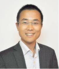
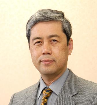
Giovanni Ghione - Editor-in-Chief
Department of Electronics and Telecommunications, Torino, Italy
Giovanni Ghione graduated cum laude in Electronic Engineering from Politecnico di Torino, Torino Italy in 1981. He was Assistant Professor in Electromagnetic Fields since 1983, Associate Professor in Circuit Theory with Politecnico di Milano, Milano Italy since 1987, and finally Full Professor in Electronics since 1990, first with University of Catania, then again with Politecnico di Torino. His research activity has been mainly concerned with high-frequency electronics and optoelectronics. He has contributed to the physics-based modelling of compound semiconductor devices, with particular interest in the numerical noise modeling in the small- and large-signal regimes, in the thermal modeling of devices and integrated circuits, and in the modeling of widegap semiconductors devices and materials. He has also done research in the field of microwave electronics, with contributions in the modeling of passive elements, in particular coplanar components, and in the design of power MMICs. Prof. Ghione was actively engaged since 1985 in research on optoelectronic devices, with application to the modeling and design of near and far-IR photodetectors, electrooptic and electroabsorption modulators, and GAN-based LEDs. Prof. Ghione has authored or co-authored more than 300 research papers on the above subjects and five books. He is an IEEE Fellow (class 2007). He has been a member of the QPC subcommitee of IEDM in 1997-1998 and in 2006-2007 and Chair in 2008; in 2009-2010 he was the EU Arrangement Co-Chair of IEDM. From 2010 to 2015 he has been chair of the EDS Committee on Compound Semiconductor Devices and Circuits. He has been Chair of the GAAS2003 conference and he has been subcommittee chair in several SCs of the European Microwave Week. He was President of the Library System of Politecnico from 1997 to 2007. From 2007 to 2015 he was the Head of the Department of Electronics and Telecommunications of Politecnico di Torino.
Publications and Products Committee Members
Joachim N. Burghartz - Fellow
Joachim N. Burghartz is an IEEE Fellow, an IEEE Distinguished Lecturer, recipient of the 2014 EDS J.J. Ebers Award, and has been an ExCom member of the IEEE Electron Devices Society. He received his MS degree from RWTH Aachen in 1982 and his PhD degree in 1987 from the University of Stuttgart, both in Germany. From 1987 thru 1998 he was with the IBM T. J. Watson Research Center in Yorktown Heights, New York, where he was engaged in early development of SiGe HBT technology and later in research on integrated passive components, particularly inductors, for application to monolithic RF circuits. From 1998 until 2005 he was with TU Delft in the Netherlands as a full professor and from 2001 as the Scientific Director of the Delft research institute DIMES. In fall 2005 he moved to Stuttgart, Germany, to head the Institute for Microelectronics Stuttgart (IMS CHIPS). In addition, he is affiliated with the University of Stuttgart as a full professor. More recently, he also became CEO of the IMS Mikro-Nano Produkte GmbH. Dr. Burghartz has published about 350 reviewed articles and holds more than 30 patents. Distinguished Lecture Titles -Hybrid Systems in Foil -Ultra-thin chip technology -GaN technologies for power and RF
Lecture Topics:
-Ultra-Thin Chips – A New Paradigm in Silicon Technology
-Hybrid Systems-in-Foil - Combining the Merits of Thin Chips and of Large-Area Electronics
-GaN-on-Si Technology for Power, RF & Specials
-Marvels of Microelectronic Engineering
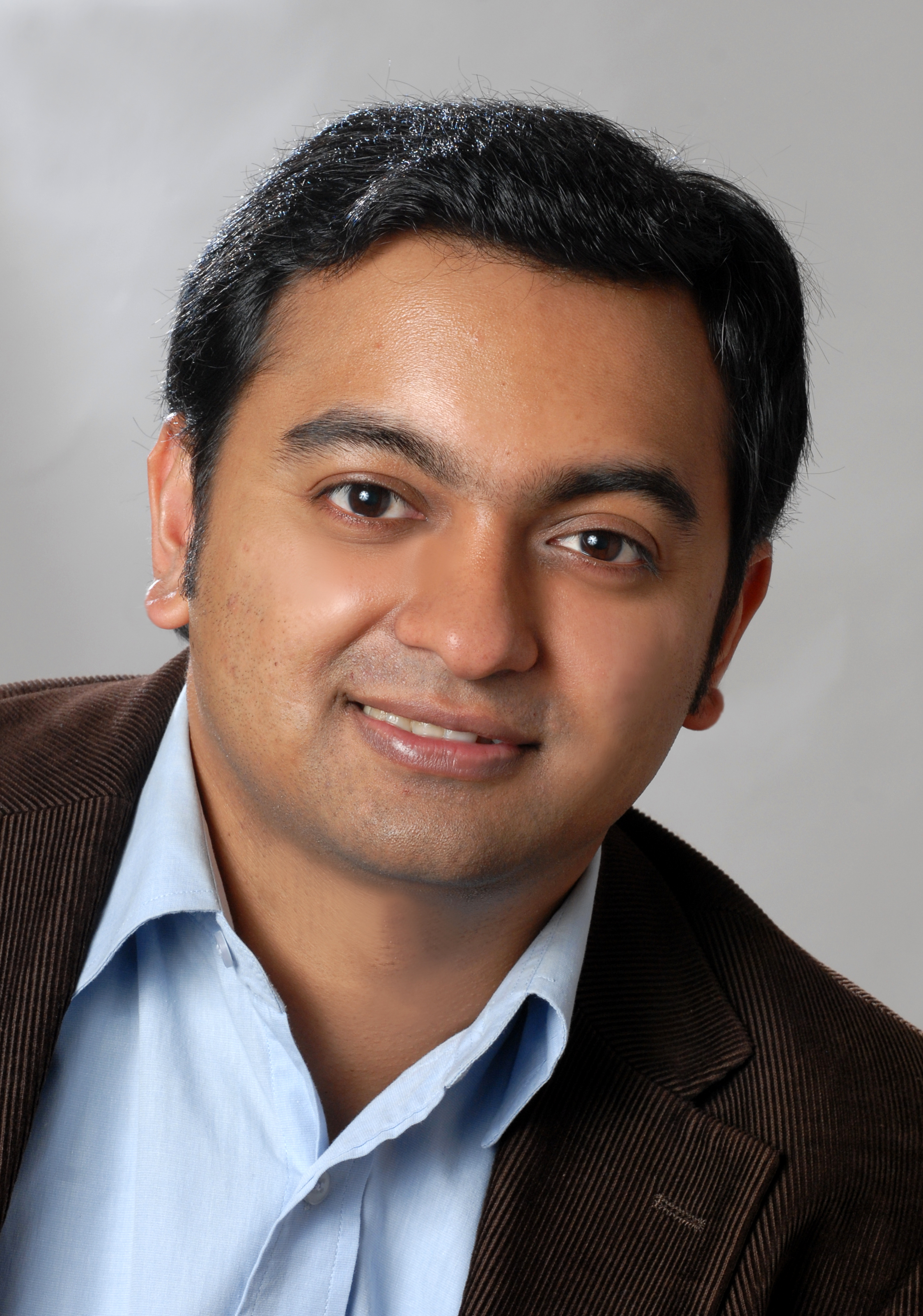
Avirup Dasgupta
Prof. Avirup Dasgupta is an assistant professor in the Dept. of Electronics and Communication Engineering at the Indian Institute of Technology Roorkee (IITR), where he leads the DiRac Lab (Device Research Lab). His work primarily involves semiconductor physics as well as the analysis, modeling and design of semiconductor devices. A major part of his group's work is developing compact models. Prof. Dasgupta is a co-developer of multiple industry standard models including BSIM-BULK, BSIM-IMG, BSIM-CMG, BSIM-SOI and ASM-HEMT. He also develops various compact models for different industry clients. Prof. Dasgupta is one of the leaders in the area of machine learning for electronic design automation. His group also works on various logic and memory devices, cryogenic device-circuit codesign, 2D materials and green energy.
Prof. Dasgupta is an IEEE Senior Member and the recipient of the IEEE EDS Early Career Award (2021). He serves as the reviewer for multiple journals and conferences and serves as a member of the IEEE EDS Compact Modeling Technical Committee, IEEE EDS Publications and Products Standing Committee and IEEE UP Section Executive Committee. Prof. Dasgupta completed his undergraduate, graduate and doctoral work at the Indian Institute of Technology Kanpur (IITK). He worked as the manager of the Berkeley Device Modeling Center (BDMC) and as a postdoctoral scholar in the BSIM group at the Dept. of Electrical Engineering and Computer Science, University of California Berkeley, prior to joining IITR.
Patrick Fay
Dept. of Electrical Engineering, IN, USA
Patrick Fay received a B.S. degree in Electrical Engineering from the University of Notre Dame in 1991, followed by the M.S. and Ph.D. degrees in Electrical Engineering from the University of Illinois at Urbana-Champaign in 1993 and 1996, respectively. He joined the faculty of the Department of Electrical Engineering at the University of Notre Dame in 1997, where he currently a professor as well as the director of the Notre Dame Nanofabrication Facility. His research interests include the design, fabrication, and characterization of III-V microwave and millimeter-wave electronic devices and circuits, power devices, and high-speed optoelectronic devices and optoelectronic integrated circuits. His research also includes the development and use of micromachining techniques for the fabrication of microwave and millimeter-wave components and packaging. Prof. Fay was awarded the Department of Electrical Engineering’s Outstanding Teacher award in 1998 and 2018, and Notre Dame's College of Engineering’s Outstanding Teacher award in 2015. He is a fellow of the IEEE, and Electron Device Society Distinguished Lecturer, and serves as an associate editor of the IEEE Transactions on Components, Packaging and Manufacturing Technology, IEEE Transactions on Electron Devices, and IEEE Transactions on Microwave Theory and Techniques.
Lecture Topics
- III-N Devices and Integration for Millimeter-Wave and Power Applications
- Vertical GaN Devices and Epitaxial Lift-Off Processing for High Performance Power Applications
- Advances in III-N Devices for Power and Internet of Things Applications
- III-N Nanowire FETs for Low-Power Applications
- Advanced Tunneling-Based Devices for mm-Wave Sensing and Imaging
Xiaojun Guo - Optoelectronics, Display, Imaging
Xiaojun Guo is now Professor in Department of Electronic Engineering at Shanghai Jiao Tong University, China. He received the Bachelor degree from Jilin University (China) in 2002, and the Ph.D. degree from University of Surrey (UK) in 2007, both in electronic engineering. He worked on EDA for VLSIs in Department of Electronic Engineering at Tsinghua University during 2002-2003. His PhD research was on system-on-panel integration with low-temperature poly-Si TFTs. Before joining Shanghai Jiao Tong University in Aug. 2009, he had been working in Plastic Logic Ltd., Cambridge, UK, on research and development of printed polymer TFTs backplanes for flexible displays, and technology transfer for manufacturing. His group at Shanghai Jiao Tong University is now focusing on device and integration of printable thin film transistors and functional devices including displays, sensors and memories. He has authored or co-authored more than 60 technical papers in international journals and conference.
Lecture Titles
-Thin-fi lm transistor for Flexible Heterogeneous Integration
-Organic thin-fi lm Transistor for Display and Sensor Integration
-Low power Flexible Hybrid Integration for IoT
-Active-Matrix Backplane Design and Integration for Advanced Displays
Francesca Iacopi

School of Electrical and Data Engineering | Faculty of Engineering & IT
Prof. Francesca Iacopi (PhD in EE, KULeuven, 2004) has 20 years’ experience in Materials and Devices for Semiconductor Technologies across industry and academia, with over 120 peer-reviewed publications and 9 granted patents. Her research emphasis is the translation of basic scientific advances in nanomaterials and novel device concepts into a wide range semiconductor technologies, covering Cu/Low-k interconnects, novel TFET devices, advanced packaging and heterogeneous integration. Research Scientist at IMEC (Belgium) over 1999-2009, she then took up a one -year Guest Professorship at the University of Tokyo (Japan). In 2010-2011 she directed the Chip-Package Interaction strategy for GLOBALFOUNDRIES (Ca, USA), before becoming full -time Academic in Australia in 2012, where she invented a process to obtain graphene on silicon wafers, with applications in integrated sensing and energy storage. She was recipient of an MRS Gold Graduate Student Award (2003), an Australian Research Council Future Fellowship (2012), and a Global Innovation Award at TechConnect in Washington DC (2014). She is a Fellow of the Institution of Engineers Australia, Senior Member IEEE and she is currently Head of Discipline, Communications and Electronics, of the Faculty of Engineering and IT at the University of Technology Sydney.
Lecture Topics
- Graphene on cubic silicon carbide: a platform on silicon for More-Than-Moore integrated technologies
Sanghun Jeon
Chen Jiang
Nripan Matthews
Arokia Nathan - Fellow
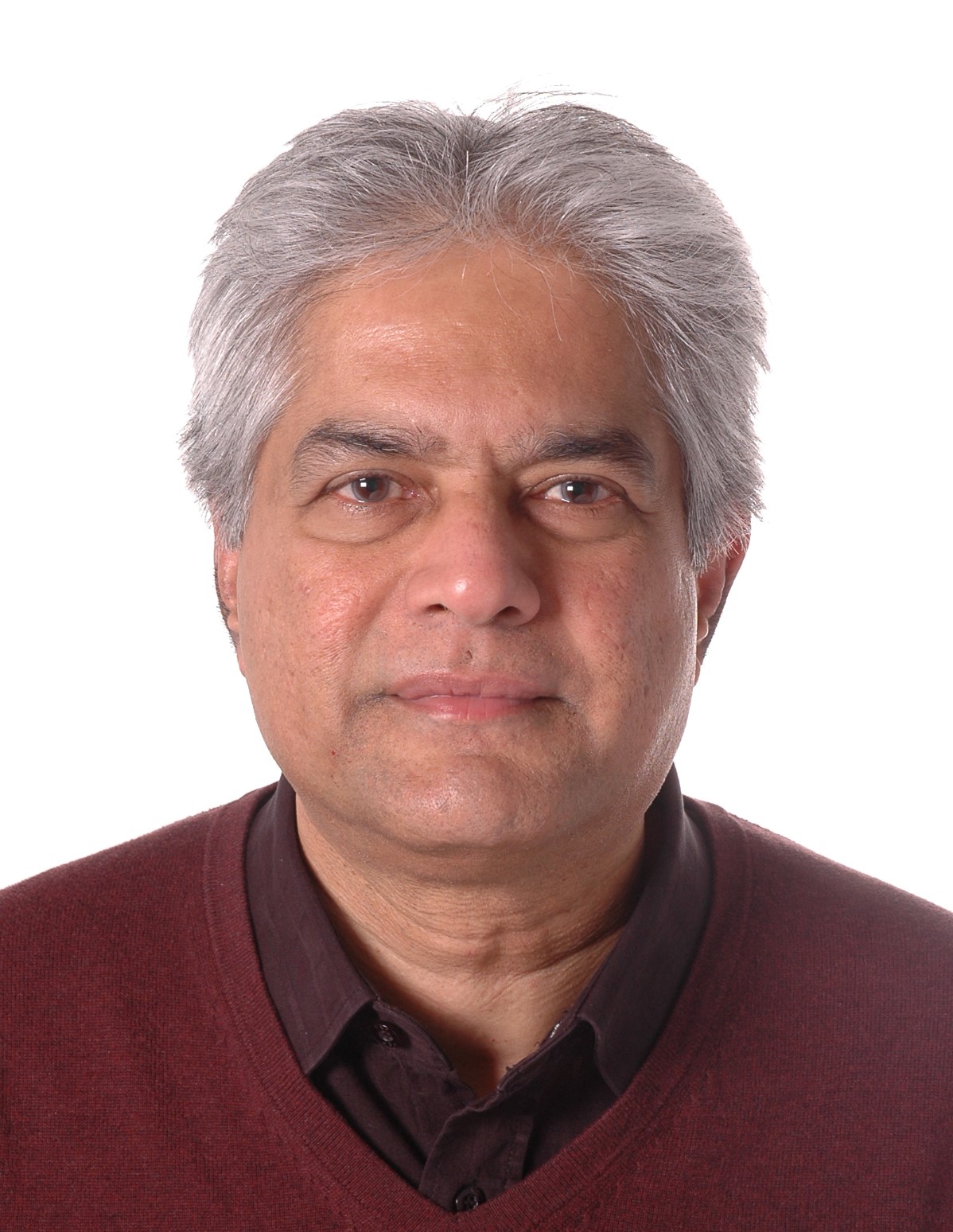
Arokia Nathan is currently a Bye-Fellow and Tutor at Darwin College, University of Cambridge, UK. He received his PhD degree in electrical engineering from the University of Alberta, Canada, in 1988. He joined LSI Logic USA, and subsequently, the Institute of Quantum Electronics, ETH Zürich, Switzerland, before joining the Electrical and Computer Engineering Department at the University of Waterloo, Canada. In 2006, he joined the London Centre for Nanotechnology, University College London, UK, as the Sumitomo Chair of Nanotechnology. He moved to Cambridge University in 2011 as the Chair of Photonic Systems and Displays. He has more than 600 publications, including six books, and more that 110 patents and four spin-off companies. He is the co-founder of Cambridge Touch Technologies, UK and VISBAN Networks UK where he is a Director and Chief Technical Officer. He is a Fellow of IEEE and SID, a Distinguished Lecturer of the IEEE Electron Devices Society and Sensor Council, a Chartered Engineer (UK), Fellow of the Institution of Engineering and Technology (UK), and winner of the 2020 IEEE EDS JJ Ebers Award.
Lecture Topics
- Flexible Electronics
- Oxide Semiconductor Electronics
- Ultralow Power Transistors and Sensor Interfaces
- Active Matrix OLED Displays
- TFT Compact Modeling and Parameter Extraction
- Nanoscale Large Area Electronics
Samar K. Saha - Life Fellow
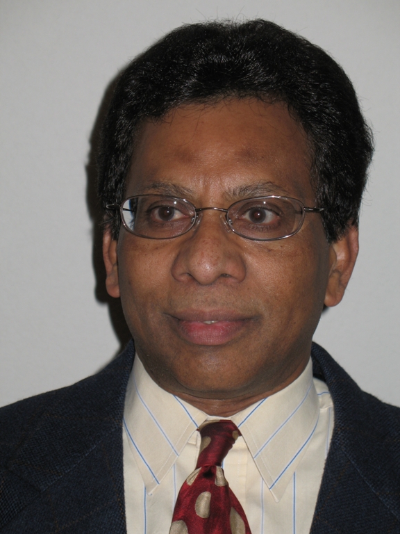
Samar Saha has served as the 2016-2017 President of the IEEE Electron Devices Society (EDS) and currently serving as the Senior Past President and Chairs of the J.J. Ebers Award and Fellow Evaluations Committees. He is the Chief Research Scientist at Prospicient Devices, California, USA and an Adjunct faculty in the Electrical Engineering (EE) department, Santa Clara University, USA. In the past, he has worked in various technical and management positions for National Semiconductor, LSI Logic, Texas Instruments, Philips Semiconductors, Silicon Storage Technology, Synopsys, DSM Solutions, Silterra USA, and SuVolta. In academia, he has worked as a faculty member in the EE departments at Southern Illinois University, Carbondale; Auburn University; the University of Nevada, Las Vegas; and the University of Colorado, Colorado Springs.
Dr. Saha has authored over 100 research papers; two books, entitled, FinFET Devices for VLSI Circuits and Systems (2020) and Compact Models for Integrated Circuit Design: Conventional Transistors and Beyond (2015); one book chapter on Technology Computer-Aided Design (TCAD); and holds 12 US patents. His research interests include exploratory device and process architectures, compact modeling, renewable energy, and R & D management. He is an IEEE Life Fellow and a Fellow of the Institution of Engineering and Technology, UK.
Lecture Topics: (1) Advanced Field-Effect Transistor Device Technologies for Ultra-low Power VLSI Circuits and Systems at Nanometer Nodes; (2) Physics of Integrated Circuit Device Models for VLSI Circuit Design; (3) Thin Film Transistors for Ubiquitous Flexible Electronics; (4) Evolution of Semiconductor Devices Enabling Smart Environments and Integrated Ecosystems.
Sayeef Salahuddin
Electrical Engineering and Computer Sciences
Sayeef Salahuddin is the TSMC Distinguished professor of Electrical Engineering and Computer Sciences at the University of California Berkeley. Salahuddin received his B.Sc.in Electrical and Electronic Engineering from BUET (Bangladesh University of Engineering and Technology) in 2003 and PhD in Electrical and Computer Engineering from Purdue University in 2007. He joined the faculty of Electrical Engineering and Computer Science at University of California, Berkeley in 2008.
His work has focused on conceptualization and exploration of novel device physics for low power electronic and spintronic devices. Salahuddin has championed the concept of using 'interacting systems' for switching, showing fundamental advantage of such systems over the conventional devices in terms of power dissipation. This led to the discovery of Negative Capacitance Transistors that allows for sub kT/q subthreshold operation in transistors.
Salahuddin has received the Presidential Early Career Award for Scientist and Engineers (PECASE), the highest honor bestowed by the US Government on early career scientist and engineers. Salahuddin also received a number of other awards including the NSF CAREER award, the IEEE Nanotechnology Early Career Award, the Young Investigator Awards from the Air Force Office of Scientific Research (AFOSR) and the Army Research Office (ARO) and best paper awards from IEEE Transactions on VLSI Systems and from the VLSI-TSA conference. In 2012, Applied Physics Letters (APL) highlighted two of his papers among 50 most notable papers among all areas published in APL within 2009-2012. Salahuddin also received the George E Smith Award from the IEEE Electron Devices Society.
Salahuddin is a co-director of the Berkeley Device Modeling Center and Berkeley Center for Negative Capacitance Transistors. He is also an associate director for the Applications and Systems-Driven Center for Energy-Efficient Integrated NanoTechnologies (ASCENT), a center jointly funded by the Semiconductor Research Corporation and DARPA within the JUMP initiative.
He served on the editorial board of IEEE Electron Devices Letters (2013-16) and was the chair the IEEE Electron Devices Society committee on Nanotechnology (2014-16).
Salahuddin is a fellow of the IEEE and the APS.
Osamu Tabata
Research Areas: (1) Micro sensors, actuators and integrated sensors, (2) Microfabrication especially etching and lithography (UV, X-ray), (3) Nanofabrication, (4) DNA nanotechnology, (5) Characterization of thin film mechanical properties
Professional Memberships: IEEE
Biography: Osamu Tabata had been with the Toyota Central Research and Development Laboratories from 1981. In 1996, he joined the Department of Mechanical Engineering, Ritsumeikan University, Japan. In 2003, he moved to Kyoto University, Japan. October 2019, he moved to Kyoto University of Advanced Science and he is serving as a Founding Dean of New Faculty of Engineering from April 2020. From September to December 2000, he was a guest Professor of Institute of Microsystem Technology, University of Freiburg, Germany, from January to March 2001, he was a guest Professor of ETH Zurich, Switzerland. He had visiting Professorship for senior international scientists of the Chinese Academy of Science in 2010. He is an external senior research fellow at Freiburg Institute for Advanced Studies (FRIAS) from May 2010 and a guest Professor of Huazong University of Science and Technology from 2011. He served as a General Chair of MEMS2003 and NEMS2012, and general co-chair of NMDC2012. Currently he is an associate editor of several Journals in the field of Nano/Microsystems and N/MEMS. Also he is serving as a program committee member of many International Conferences. He is interested in the research to realize a unique and novel nanosystem by assembling the various functional components such as a microchip, a particle, a microcapsule, DNA origami, a cell, etc., with sizes ranging from the nanometer to micrometer scale on a few mm square MEMS substrate.
Ravi M. Todi
Ravi Todi received his M.S. degree in Electrical and Mechanical Engineering from University of Central Florida in 2004 and 2005 respectively, and his doctoral degree in Electrical Engineering in 2007. His graduate research work was focused on gate stack engineering, with emphasis on binary metal alloys as gate electrode and on high mobility Ge channel devices. In 2007 he started working as Advisory Engineer/Scientist at Semiconductor Research and Development Center at IBM Microelectronics Division focusing on high performance eDRAM integration on 45nm SOI logic platform. Starting in 2010 Ravi was appointed the lead Engineer for 22nm SOI eDRAM development. For his many contributions to the success of eDRAM program at IBM, Ravi was awarded IBM’s Outstanding Technical Achievement Award in 2011. Ravi Joined Qualcomm in 2012, responsible for 20nm technology and product development as part of Qualcomm’s foundry engineering team. Ravi is also responsible for early learning on 16/14 nm FinFet technology nodes. Ravi had authored or co-authored over 50 publications, has several issues US patents and over 25 pending disclosures.
Lecuture Topic
- MOS Devices and Technology
Florin Udrea - Solid-State Power and High-Voltage Devices
Florin Udrea is a professor in semiconductor engineering and head of the High Voltage Microelectronics and Sensors Laboratory at University of Cambridge. He received his BSc from University of Bucharest, Romania in 1991, an MSc in smart sensors from the University of Warwick, UK, in 1992 and the PhD degree in power devices from the University of Cambridge, Cambridge, UK, in 1995. Since October 1998, Prof. Florin Udrea has been an academic with the Department of Engineering, University of Cambridge, UK. Between August 1998 and July 2003 he was an advanced EPSRC Research Fellow and prior to this, a College Fellow in Girton College, University of Cambridge. He is currently leading a research group in power semiconductor devices and solid-state sensors that has won an international reputation during the last 20 years. Prof. Udrea has published over 350 papers in journals and international conferences. He holds 70 patents with 20 more patent applications in power semiconductor devices and sensors. Prof. Florin Udrea co-founded three companies, Cambridge Semiconductor (Camsemi) in power ICs, Cambridge CMOS Sensors (CCS) in the field of smart sensors and Cambridge Microelectronics in Power Devices. Prof. Florin Udrea is a board director in Cambridge Enterprise. For his ‘outstanding personal contribution to British Engineering’ he has been awarded the Silver Medal from the Royal Academy of Engineering.
Man Wong - EIC
Hong Kong
Research Areas: Fabrication technology and physical MEMS devices
Professional Memberships: IEEE, SID
Biography: Man Wong was born in Beijing, China. From 1979 to 1984, he studied at the Massachusetts Institute of Technology, USA, where he obtained his BS and MS degrees in Electrical Engineering. From 1985 to 1988, he was at the Center for Integrated Systems at Stanford University, USA, where he worked on tungsten-gate MOS technology and obtained his PhD degree, also in Electrical Engineering. From 1988 to 1992, he was with the Semiconductor Process and Design Center of Texas Instruments, USA and worked on the modeling and development of integrated-circuit metallization systems and dry/vapor surface-conditioning processes. He is currently with the Department of Electronic and Computer Engineering at the Hong Kong University of Science and Technology, Hong Kong. His research interests include micro-fabrication technology, device structure and material; physics and technology of thin-film transistor; organic light-emitting diode display technology; modeling and implementation of integrated micro-systems; and thin-film solar cell device and process technology. He is a member of Tau Beta Pi, Eta Kappa Nu and Sigma Xi. He was appointed an Honorary Guest Professor of Nankai University, Tianjin, China, in 2003 and a Visiting Professor of Soochow University, Suzhou, China, in 2011.
Bin Zhao - Fellow
Lecture Topics:
- Analog/Mixed-Signal/RF IC and Enabling Technologies
- High Performance VLSI Interconnect
- About EDS
- Mission, Vision and Field of Interest Statements
- Mission Fund
- Strategic Directions
- Governance
- EDS Constitution
- EDS Bylaws
- EDS Charters
- EDS Roster
- Governance Meeting
- Board of Governors & Officer Election
- ExCom
- BoG Elected Members-at-Large
- Standing Committees
- Awards Committee
- Communications Committee
- Educational Activities Committees
- Fellow Evaluations
- Finance Committee
- Humanitarian Committee
- Meetings Committee
- Membership Committee
- Newsletter Oversight Committee
- Nominations & Elections Committee
- Publications and Products Committee
- Regions & Chapters Committee
- Strategic Directions Committee
- Ad hoc Committees
- Publication Representatives
- IEEE Committee Representatives
- Past Presidents
- Voting Forum
- EDS Executive Office
- Volunteer Resources
- EDS Overview Slides
- EDS Humanitarian / Special Projects
- EDS Society Brief
- EDS 50th Anniversary Booklet
- 75th Anniversary of the Transistor
- Sitemap
- EDS Communications
