- Home
- About EDS
- Governance
- Ad hoc Committees
Ad hoc Committees
Fundraising Ad hoc Committee Chair
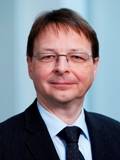
Meikei Ieong - Fellow

Chief Technology Officer
Biography: Meikei Ieong (SM’01) received the B.S. degree in electrical engineering from the National Taiwan University, Taipei, Taiwan, in 1991 and the M.S. and Ph.D. degrees in electrical and computer engineering from the University of Massachusetts, Amherst, in 1993 and 1996, respectively. He also received an MBA degree from the Sloan Fellows Program of Massachusetts Institute of Technology in 2013.
Meikei is currently Vice-President of TSMC Europe. He was program director of TSMC’s 28nm High-Performance and Mobile Technologies. Prior to that he held various engineering and management positions at IBM including senior manager at IBM TJ. Watson Research Center, Yorktown, NY. He’s recipient of IBM Technical Achievement and Corporate awards and was elected as a Master Inventor at IBM Research.
He held an adjunct associate professor position with the Department of Electrical Engineering from the Columbia University, NY in 2001. He was General Chairman of the IEEE International Electron Devices Meeting (IEDM). He has served as an editor for the IEEE Transaction on Electron Devices since 2010 and as chair of the IEEE EDS Education Award committee since 2013. He has Published more than one hundred papers in referred journals and conference proceedings and more than eighty patents. He also speaks frequently at international conferences and seminars.
Fundraising Ad hoc Committee Member
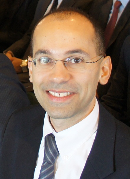
Ravi M. Todi
Ravi Todi received his M.S. degree in Electrical and Mechanical Engineering from University of Central Florida in 2004 and 2005 respectively, and his doctoral degree in Electrical Engineering in 2007. His graduate research work was focused on gate stack engineering, with emphasis on binary metal alloys as gate electrode and on high mobility Ge channel devices. In 2007 he started working as Advisory Engineer/Scientist at Semiconductor Research and Development Center at IBM Microelectronics Division focusing on high performance eDRAM integration on 45nm SOI logic platform. Starting in 2010 Ravi was appointed the lead Engineer for 22nm SOI eDRAM development. For his many contributions to the success of eDRAM program at IBM, Ravi was awarded IBM’s Outstanding Technical Achievement Award in 2011. Ravi Joined Qualcomm in 2012, responsible for 20nm technology and product development as part of Qualcomm’s foundry engineering team. Ravi is also responsible for early learning on 16/14 nm FinFet technology nodes. Ravi had authored or co-authored over 50 publications, has several issues US patents and over 25 pending disclosures.
Lecuture Topic
- MOS Devices and Technology
H.S. Philip Wong - Fellow
Lecture Topics: Nanoscale Devices and Fabrication
Paul K.L. Yu - Fellow
ECE Department, MS 0407
Lecture Topics:
- Recent Advances in Photonic Devices for RF/Wireless
- Semiconductor Wafer Bonding Technology for Device Integration
- Green Campus projects
Bin Zhao - Fellow
Lecture Topics:
- Analog/Mixed-Signal/RF IC and Enabling Technologies
- High Performance VLSI Interconnect
EDS Newsletter New Directions Ad Hoc Committee Chair
M.K. Radhakrishnan - Life Senior Member
MK Radhakrishnan (M’82, SM’94, LSM’18) is the Founder Director of NanoRel LLP -Technical Consultants providing analysis-based solutions to micro and nano electronic industries for improving reliability of devices. As a researcher in the area of semiconductor device failure physics for more than 35 years, he worked with industries (ST Microelectronic and Philips), research institutions (Institute of Microelectronics, Singapore and Indian Space Research Organization) and in academia with National University of Singapore. As a technical consultant he works with many MNCs and also provides training on device failure analysis & reliability to various Industries, Universities and Research Centres.
Lecture Topics:
- Circa 70 – Semiconductor Device Progression and Challenges towards Nanoera.
- Interface Physics and Analysis Challenges in Silicon Nanodevices
- Are the Progressions towards the “Benefit of Humanity”? - A Failure Analyst’s View
EDS Newsletter New Directions Ad Hoc Committee Member
Karim S. Karim - Senior Member
Lecture Topics:
1. Low dose digital X-ray imagers in large area thin film technology
2. High resolution digital imagers using hybrid CMOS technology
3. Enabling single photon counting with amorphous semiconductors
Biography
Karim S. Karim holds a PhD (2002) in Electrical and Computer Engineering from the University of Waterloo and an MBA (2012) from the University of Toronto. He is currently a Full Professor in the Faculty of Engineering at the University of Waterloo in Canada. In 2012, while on sabbatical, Dr. Karim spent eight months as the Head of Academic Planning at the University of Central Asia (Bishkek, Kyrgyzstan). Dr. Karim is a Senior Member of the Institute for Electrical and Electronics Engineers (IEEE), a Full Member of the American Association of Physicists in Medicine, and is a registered Professional Engineer in Canada. Dr. Karim also serves as the Associate Director for the Centre for Bioengineering and Biotechnology at the University of Waterloo, a university wide center he helped found that bridges the gap between Science and Engineering interdisciplinary research.
Joao Martino - Senior Member
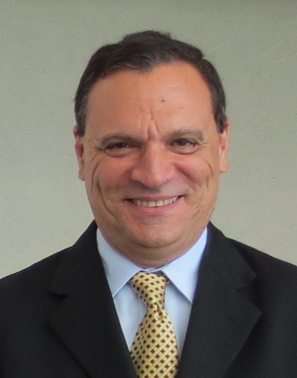
Joao Antonio Martino received master (1984) and PhD (1988) degrees in microelectronics from University of Sao Paulo, Brazil. He was a postdoctoral researcher in silicon-on-insulator (SOI) devices and technology in Imec, Belgium. He is currently a full professor and the head of SOI group at University of Sao Paulo. His expertise is in electrical characterization, simulation and modeling of SOI devices in wide temperature range. He is also interested in the SOI-CMOS fabrication process, multiple-gate devices (FinFET), 1T-DRAM, Tunnel-FET and radiation effects. He has authored or coauthored of more than 400 technical journal papers and conference presentation and author/editor of 5 books. He is senior member and distinguished lecturer of the IEEE Electron Device Society (EDS). He is chair of IEEE/EDS South Brazil chapter and vice-chair of SRC IEEE/EDS R9.
Lecture Topics:
-Field Effect Transistor: From MOSFET to Tunnel FET
-Transistor Evolution; From Micro to Nano Era
-Tunnel FET Transistors (triple-gate and nanowire structures)
-Radiation effects on SOI devices (planar and multiple gates devices)
-SOI MOSFET: Electrical Characterization and Modeling
-Circuit Simulation using Verilog A approach.
Murty Polavarapu
Mail Stop MVA01-016
Samar K. Saha - Life Fellow
Samar Saha has served as the 2016-2017 President of the IEEE Electron Devices Society (EDS) and currently serving as the Senior Past President and Chairs of the J.J. Ebers Award and Fellow Evaluations Committees. He is the Chief Research Scientist at Prospicient Devices, California, USA and an Adjunct faculty in the Electrical Engineering (EE) department, Santa Clara University, USA. In the past, he has worked in various technical and management positions for National Semiconductor, LSI Logic, Texas Instruments, Philips Semiconductors, Silicon Storage Technology, Synopsys, DSM Solutions, Silterra USA, and SuVolta. In academia, he has worked as a faculty member in the EE departments at Southern Illinois University, Carbondale; Auburn University; the University of Nevada, Las Vegas; and the University of Colorado, Colorado Springs.
Dr. Saha has authored over 100 research papers; two books, entitled, FinFET Devices for VLSI Circuits and Systems (2020) and Compact Models for Integrated Circuit Design: Conventional Transistors and Beyond (2015); one book chapter on Technology Computer-Aided Design (TCAD); and holds 12 US patents. His research interests include exploratory device and process architectures, compact modeling, renewable energy, and R & D management. He is an IEEE Life Fellow and a Fellow of the Institution of Engineering and Technology, UK.
Lecture Topics: (1) Advanced Field-Effect Transistor Device Technologies for Ultra-low Power VLSI Circuits and Systems at Nanometer Nodes; (2) Physics of Integrated Circuit Device Models for VLSI Circuit Design; (3) Thin Film Transistors for Ubiquitous Flexible Electronics; (4) Evolution of Semiconductor Devices Enabling Smart Environments and Integrated Ecosystems.
Manoj Saxena - Senior Member
University of Delhi
Manoj Saxena is an Associate Professor in Department of Electronics, Deen Dayal Upadhyaya College, University of Delhi, New Delhi, India. He received B.Sc. (with honors), M. Sc., and Ph.D. degrees from the University of Delhi in 1998, 2000, and 2006 respectively. He has authored or coauthored 210 technical papers in international journals and various international and national conferences. His current research interests are in the areas of analytical modeling, design, and simulation of Optically controlled MESFET/MOSFET, silicon-on-nothing, insulated-shallow-extension, grooved/concave-gate MOSFETs, cylindrical gate MOSFET and Tunnel FET. He is a reviewer to many journals including Solid State Electronics, Journal of Physics: D Applied Physics and IEEE TED and EDL. Manoj is a Senior Member of IEEE and also Member of Institute of Physics (UK), Institution of Engineering and Technology (UK), National Academy of Sciences India (NASI) and International Association of Engineers (Hong Kong). Currently, he is the Secretary of EDS Delhi Chapter. For his voluntary contribution, Manoj received the outstanding EDS Volunteer recognition from EDS Chapters in the region in 2012.
Lecture Topics:
-Dielectric Pocket MOSFET: A Novel Device Architecture;
-Embedded Insulator based Novel Nanoscaled Novel MOSFET Structures Tunnel Field Effect Transistor and its Application as Highly Sensitive and Fast Biosensor
-Modeling and Simulation of Tunnel Field Effect Transistor Dual Material Junctionless Double Gate Transistor for Analog and Digital Performance
-Optimization of Asymmetric (Pi)π-Gate HEMT for Improved Reliability & Frequency Applications
Jonathan Terry
School of Engineering
Jonathan Terry is a Senior Member of the IEEE and the Treasurer of the Scottish Chapter of the IEEE Electron Devices Society. He is a senior research fellow at the University of Edinburgh in the Institute for Integrated Micro and Nano Systems and an honorary research fellow at Heriot-Watt University. His research centres on the development of More-than-Moore application. This is the integration of novel materials and processing techniques with standard foundry-produced CMOS technology. Jonathan also teaches within the Universityâ
Daniel Tomaszewski
D.Tomaszewski (M’2014) received M.Sc degree in electronics (spec. electronic technology) from Warsaw University of Technology in 1980, and Ph.D degree in electrical engineering (spec. solid-state device electronics) from Instytut Technologii Elektronowej, Warsaw in 1998.
EDS Conference Platform Ad Hoc Committee Chair
Can Li
EDS Conference Platform Ad Hoc Committee Member
Yang Chai - Senior Member
Dr. Yang Chai received his PhD degree from the Hong Kong University of Science and Technology in 2009. After he conducted his Postdoctoral studies at Stanford University and University of Illinois at Urbana & Champaign, he joined the Department of Applied Physics in the Hong Kong Polytechnic University in 2012. He is a recipient of RGC Early Career Award in 2014, and the Semiconductor Science and Technology Early Career Research Award in 2017. His current research interest includes low-dimensional material for electron devices.
Lecture Topics:
- Two-dimensional layered materials for nanoelectronics
- Neuromophric computing and sensing based on emerging memories
Muyuan Peng
Keyi Shan
Bo Wen
EDS Conference Event Finance Ad Hoc Committee Chair
Roger Booth
EDS Conference Event Finance Ad Hoc Committee Member
Shuji Ikeda
NIRC
Shuji Ikeda (M’91-SM’02-F’04) received the B.S. degree in Physics, PhD. in Electrical Engineering from Tokyo Institute of Technology, Tokyo, Japan in 1978 and 2003 respectively and the M.S. degree in Electrical Engineering from Princeton University, Princeton, New Jersey, USA in 1987. He joined Semiconductor and Integrated Circuit Group, Hitachi ltd., Tokyo, Japan in 1978, where he was engaged in research and development of state of the art SRAM process and devices. He was also working on developing process technology for LOGIC, embedded memories, and CMOS power RF devices and on transferring technology to mass production line. He invented some of the outstanding structures for SRAM. He pioneered process to implement new materials in mass production, including W-polycide, Al-Cu-Si in 1984 and in-situ phosphorus-doped-polysilicon in 1990. He is the first to realize Lightly Doped Drain (LDD) in production to suppress Hot Carrier Injection in 1984. He also firstly implemented polyimide coat of the chip to immune SER caused by alpha particle from the resin covers the chip. In October 2000, he joined Trecenti Technologies Inc. He developed new process scheme with aggressive reduction of process time and suitable for single-wafer processing. That achieved less than 0.25days/layer cycle time. In April 2005, he joined ATDF at Austin Texas, as a Director of Technology. Where he develops various kinds of technologies includes scaled CMOS, non-classical CMOS, new materials and tools. He established tei Technology LLC in May 2008, Omni Water Solutions LLC, in 2009 at Austin Texas. He started tei Solutions Inc in Tsukuba, Ibaraki, Japan in 2010, where, he manages R&D foundry developing new devices, process technologies for VLSIs. He also integrates emerging technology onto semiconductor manufacturing technology to create innovative products/businesses. Due to his contributions to 200 MHz RISC microprocessor, he got 1999 R&D 100 Award. He served as subcommittee and executive committee member of IEDM from 1993 to 2002. He introduced Manufacturing Session in 1998 and chaired IEDM in 2002. He was a member of EDS Administrative Committee from 2005 to 2010. He was a technical program member for VLSI Technology Symposium in 2007 and 2008. He serves as a chairman of VLSI committee of EDS from 2009 and AdHoc Committee on Asia EDS Conference from 2014.
Masumi Saito
Ravi M. Todi
Ravi Todi received his M.S. degree in Electrical and Mechanical Engineering from University of Central Florida in 2004 and 2005 respectively, and his doctoral degree in Electrical Engineering in 2007. His graduate research work was focused on gate stack engineering, with emphasis on binary metal alloys as gate electrode and on high mobility Ge channel devices. In 2007 he started working as Advisory Engineer/Scientist at Semiconductor Research and Development Center at IBM Microelectronics Division focusing on high performance eDRAM integration on 45nm SOI logic platform. Starting in 2010 Ravi was appointed the lead Engineer for 22nm SOI eDRAM development. For his many contributions to the success of eDRAM program at IBM, Ravi was awarded IBM’s Outstanding Technical Achievement Award in 2011. Ravi Joined Qualcomm in 2012, responsible for 20nm technology and product development as part of Qualcomm’s foundry engineering team. Ravi is also responsible for early learning on 16/14 nm FinFet technology nodes. Ravi had authored or co-authored over 50 publications, has several issues US patents and over 25 pending disclosures.
Lecuture Topic
- MOS Devices and Technology
Bin Zhao - Fellow
Lecture Topics:
- Analog/Mixed-Signal/RF IC and Enabling Technologies
- High Performance VLSI Interconnect
EDS Speciality Conference Ad Hoc Committee Chair
Hiro Akinaga
EDS Speciality Conference Ad Hoc Committee Member
John Dallesasse
University of Illinois at Urbana-Champaign
John Dallesasse is a Professor of Electrical and Computer Engineering and Associate Dean in the Grainger College of Engineering at the University of Illinois at Urbana-Champaign, where he’s been for over 10 years. He also has over 20 years of industry experience in technology development and executive management, having led technically diverse and geographically distributed engineering teams. Prior to joining UIUC he was the Chief Technology Officer, Vice President, and co-founder of Skorpios Technologies where he was responsible for developing innovative methods for heterogeneous integration of compound semiconductors with silicon. His technical contributions include, with Nick Holonyak, Jr., the discovery of III‑V Oxidation, which has become an enabling process technology for the fabrication of Vertical-Cavity Surface-Emitting Lasers (VCSELs) for optical networking, 3D imaging, and LIDAR applications. John has over 100 publications and conference presentations, and 50 issued patents. He serves as the Chair of the Steering Committee for the IEEE Journal of Lightwave Technology, the Chair of the Steering Committee for the IEEE Transactions on Semiconductor Manufacturing, and as the Vice President of Technical Committees for IEEE-EDS. He is a Fellow of the IEEE and Optica.
Christofer Hierold
Micro and Nanosystems
Research Areas:Functional nanomaterials in MEMS and NEMS (e.g. carbon nanotube sensors, ultra low power sensors), Polymer microsystems (e.g. magnetic polymers, biodegradable polymers), Advanced MEMS (e.g. micro thermoelectric generators, large deflection actuators by polymer springs in MEMS),Fabrication technology (integration of functional nanomaterials on larger areas)
Professional Memberships: IEEE/EDS
Biography: Christofer Hierold has been Professor of Micro and Nanosystems at the Swiss Federal Institute of Technology in Zurich (ETH) since April 2002. Further, he is Executive Coordinator ETH Zurich of the Binnig and Rohrer Nanotechnology Center (BRNC) atRuschlikon. Before he joined ETH Zurich in 2002 he was with Siemens AG, Corporate Research, and Infineon Technologies AG in Germany. In 1990 he graduated from Technical University Munich (TUM) with a Dr.-Ing. Degree in Engineering Sciences.
Christofer Hierold is Co-Chair of the Steering Committee of the EUROSENSORS conference, and a member of the Steering Committees of both MEMS and TRANSDUCERS. He served as General Co-Chair of MEMS 2009, and is Program Chair of TRANSDUCERS 2013. Professor Hierold is a member of the Swiss Academy of Engineering Sciences (SATW).
Shuji Ikeda
NIRC
Shuji Ikeda (M’91-SM’02-F’04) received the B.S. degree in Physics, PhD. in Electrical Engineering from Tokyo Institute of Technology, Tokyo, Japan in 1978 and 2003 respectively and the M.S. degree in Electrical Engineering from Princeton University, Princeton, New Jersey, USA in 1987. He joined Semiconductor and Integrated Circuit Group, Hitachi ltd., Tokyo, Japan in 1978, where he was engaged in research and development of state of the art SRAM process and devices. He was also working on developing process technology for LOGIC, embedded memories, and CMOS power RF devices and on transferring technology to mass production line. He invented some of the outstanding structures for SRAM. He pioneered process to implement new materials in mass production, including W-polycide, Al-Cu-Si in 1984 and in-situ phosphorus-doped-polysilicon in 1990. He is the first to realize Lightly Doped Drain (LDD) in production to suppress Hot Carrier Injection in 1984. He also firstly implemented polyimide coat of the chip to immune SER caused by alpha particle from the resin covers the chip. In October 2000, he joined Trecenti Technologies Inc. He developed new process scheme with aggressive reduction of process time and suitable for single-wafer processing. That achieved less than 0.25days/layer cycle time. In April 2005, he joined ATDF at Austin Texas, as a Director of Technology. Where he develops various kinds of technologies includes scaled CMOS, non-classical CMOS, new materials and tools. He established tei Technology LLC in May 2008, Omni Water Solutions LLC, in 2009 at Austin Texas. He started tei Solutions Inc in Tsukuba, Ibaraki, Japan in 2010, where, he manages R&D foundry developing new devices, process technologies for VLSIs. He also integrates emerging technology onto semiconductor manufacturing technology to create innovative products/businesses. Due to his contributions to 200 MHz RISC microprocessor, he got 1999 R&D 100 Award. He served as subcommittee and executive committee member of IEDM from 1993 to 2002. He introduced Manufacturing Session in 1998 and chaired IEDM in 2002. He was a member of EDS Administrative Committee from 2005 to 2010. He was a technical program member for VLSI Technology Symposium in 2007 and 2008. He serves as a chairman of VLSI committee of EDS from 2009 and AdHoc Committee on Asia EDS Conference from 2014.
Kazunari Ishimaru
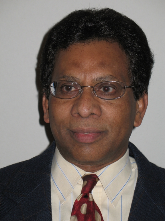
Arokia Nathan - Fellow
Arokia Nathan is currently a Bye-Fellow and Tutor at Darwin College, University of Cambridge, UK. He received his PhD degree in electrical engineering from the University of Alberta, Canada, in 1988. He joined LSI Logic USA, and subsequently, the Institute of Quantum Electronics, ETH Zürich, Switzerland, before joining the Electrical and Computer Engineering Department at the University of Waterloo, Canada. In 2006, he joined the London Centre for Nanotechnology, University College London, UK, as the Sumitomo Chair of Nanotechnology. He moved to Cambridge University in 2011 as the Chair of Photonic Systems and Displays. He has more than 600 publications, including six books, and more that 110 patents and four spin-off companies. He is the co-founder of Cambridge Touch Technologies, UK and VISBAN Networks UK where he is a Director and Chief Technical Officer. He is a Fellow of IEEE and SID, a Distinguished Lecturer of the IEEE Electron Devices Society and Sensor Council, a Chartered Engineer (UK), Fellow of the Institution of Engineering and Technology (UK), and winner of the 2020 IEEE EDS JJ Ebers Award.
Lecture Topics
- Flexible Electronics
- Oxide Semiconductor Electronics
- Ultralow Power Transistors and Sensor Interfaces
- Active Matrix OLED Displays
- TFT Compact Modeling and Parameter Extraction
- Nanoscale Large Area Electronics
Ravi M. Todi
Ravi Todi received his M.S. degree in Electrical and Mechanical Engineering from University of Central Florida in 2004 and 2005 respectively, and his doctoral degree in Electrical Engineering in 2007. His graduate research work was focused on gate stack engineering, with emphasis on binary metal alloys as gate electrode and on high mobility Ge channel devices. In 2007 he started working as Advisory Engineer/Scientist at Semiconductor Research and Development Center at IBM Microelectronics Division focusing on high performance eDRAM integration on 45nm SOI logic platform. Starting in 2010 Ravi was appointed the lead Engineer for 22nm SOI eDRAM development. For his many contributions to the success of eDRAM program at IBM, Ravi was awarded IBM’s Outstanding Technical Achievement Award in 2011. Ravi Joined Qualcomm in 2012, responsible for 20nm technology and product development as part of Qualcomm’s foundry engineering team. Ravi is also responsible for early learning on 16/14 nm FinFet technology nodes. Ravi had authored or co-authored over 50 publications, has several issues US patents and over 25 pending disclosures.
Lecuture Topic
- MOS Devices and Technology
Bin Zhao - Fellow
Lecture Topics:
- Analog/Mixed-Signal/RF IC and Enabling Technologies
- High Performance VLSI Interconnect
Ad Hoc on EDS Organization Enhancement Chair
Cary Y. Yang - Life Fellow
Center for Nanostructures
Cary Y. Yang received the B.S., M.S., and Ph.D. degrees in electrical engineering from the University of Pennsylvania. After working at M.I.T., NASA Ames Research Center, and Stanford University on electronic properties of nanostructure surfaces and interfaces, he founded Surface Analytic Research, a Silicon Valley company focusing on sponsored research projects covering various applications of surfaces and nanostructures. He joined Santa Clara University in 1983 and is currently Professor of Electrical Engineering and Director of TENT Laboratory, a SCU facility located inside NASA Ames. He was the Founding Director of Microelectronics Laboratory and Center for Nanostructures, and served as Chair of Electrical Engineering and Associate Dean of Engineering at Santa Clara. His research spans from silicon-based nanoelectronics to nanostructure interfaces in electronic, biological, and energy-storage systems. An IEEE Life Fellow, he served as Editor of the IEEE Transactions on Electron Devices, President of the IEEE Electron Devices Society, and elected member of the IEEE Board of Directors. He was appointed Vice Chair of the IEEE Awards Board in 2013 and 2014. He received the 2004 IEEE Educational Activities Board Meritorious Achievement Award in Continuing Education "for extensive and innovative contributions to the continuing education of working professionals in the field of micro/nanoelectronics," and the IEEE Electron Devices Society Distinguished Service Award in 2005. From 2008 to 2013, he held the Bao Yugang Chair Professorship at Zhejiang University in China.
Lecture Topics:
- Nanocarbon Interconnects
- CNT-graphene interface
Ad Hoc on EDS Organization Enhancement Member
John Dallesasse
University of Illinois at Urbana-Champaign
John Dallesasse is a Professor of Electrical and Computer Engineering and Associate Dean in the Grainger College of Engineering at the University of Illinois at Urbana-Champaign, where he’s been for over 10 years. He also has over 20 years of industry experience in technology development and executive management, having led technically diverse and geographically distributed engineering teams. Prior to joining UIUC he was the Chief Technology Officer, Vice President, and co-founder of Skorpios Technologies where he was responsible for developing innovative methods for heterogeneous integration of compound semiconductors with silicon. His technical contributions include, with Nick Holonyak, Jr., the discovery of III‑V Oxidation, which has become an enabling process technology for the fabrication of Vertical-Cavity Surface-Emitting Lasers (VCSELs) for optical networking, 3D imaging, and LIDAR applications. John has over 100 publications and conference presentations, and 50 issued patents. He serves as the Chair of the Steering Committee for the IEEE Journal of Lightwave Technology, the Chair of the Steering Committee for the IEEE Transactions on Semiconductor Manufacturing, and as the Vice President of Technical Committees for IEEE-EDS. He is a Fellow of the IEEE and Optica.
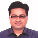
Murty Polavarapu
Mail Stop MVA01-016
Ravi M. Todi
Ravi Todi received his M.S. degree in Electrical and Mechanical Engineering from University of Central Florida in 2004 and 2005 respectively, and his doctoral degree in Electrical Engineering in 2007. His graduate research work was focused on gate stack engineering, with emphasis on binary metal alloys as gate electrode and on high mobility Ge channel devices. In 2007 he started working as Advisory Engineer/Scientist at Semiconductor Research and Development Center at IBM Microelectronics Division focusing on high performance eDRAM integration on 45nm SOI logic platform. Starting in 2010 Ravi was appointed the lead Engineer for 22nm SOI eDRAM development. For his many contributions to the success of eDRAM program at IBM, Ravi was awarded IBM’s Outstanding Technical Achievement Award in 2011. Ravi Joined Qualcomm in 2012, responsible for 20nm technology and product development as part of Qualcomm’s foundry engineering team. Ravi is also responsible for early learning on 16/14 nm FinFet technology nodes. Ravi had authored or co-authored over 50 publications, has several issues US patents and over 25 pending disclosures.
Lecuture Topic
- MOS Devices and Technology
Bin Zhao - Fellow
Lecture Topics:
- Analog/Mixed-Signal/RF IC and Enabling Technologies
- High Performance VLSI Interconnect
