Strategic Directions Committee
Strategic Directions Committee Chair
John Dallesasse is a Professor of Electrical and Computer Engineering and Associate Dean in the Grainger College of Engineering at the University of Illinois at Urbana-Champaign, where he’s been for over 10 years. He also has over 20 years of industry experience in technology development and executive management, having led technically diverse and geographically distributed engineering teams. Prior to joining UIUC he was the Chief Technology Officer, Vice President, and co-founder of Skorpios Technologies where he was responsible for developing innovative methods for heterogeneous integration of compound semiconductors with silicon. His technical contributions include, with Nick Holonyak, Jr., the discovery of III‑V Oxidation, which has become an enabling process technology for the fabrication of Vertical-Cavity Surface-Emitting Lasers (VCSELs) for optical networking, 3D imaging, and LIDAR applications. John has over 100 publications and conference presentations, and 50 issued patents. He serves as the Chair of the Steering Committee for the IEEE Journal of Lightwave Technology, the Chair of the Steering Committee for the IEEE Transactions on Semiconductor Manufacturing, and as the Vice President of Technical Committees for IEEE-EDS. He is a Fellow of the IEEE and Optica.
Strategic Directions Non-Voting Member
Lecture Topics:
- Analog/Mixed-Signal/RF IC and Enabling Technologies
- High Performance VLSI Interconnect
Strategic Directions Committee Member
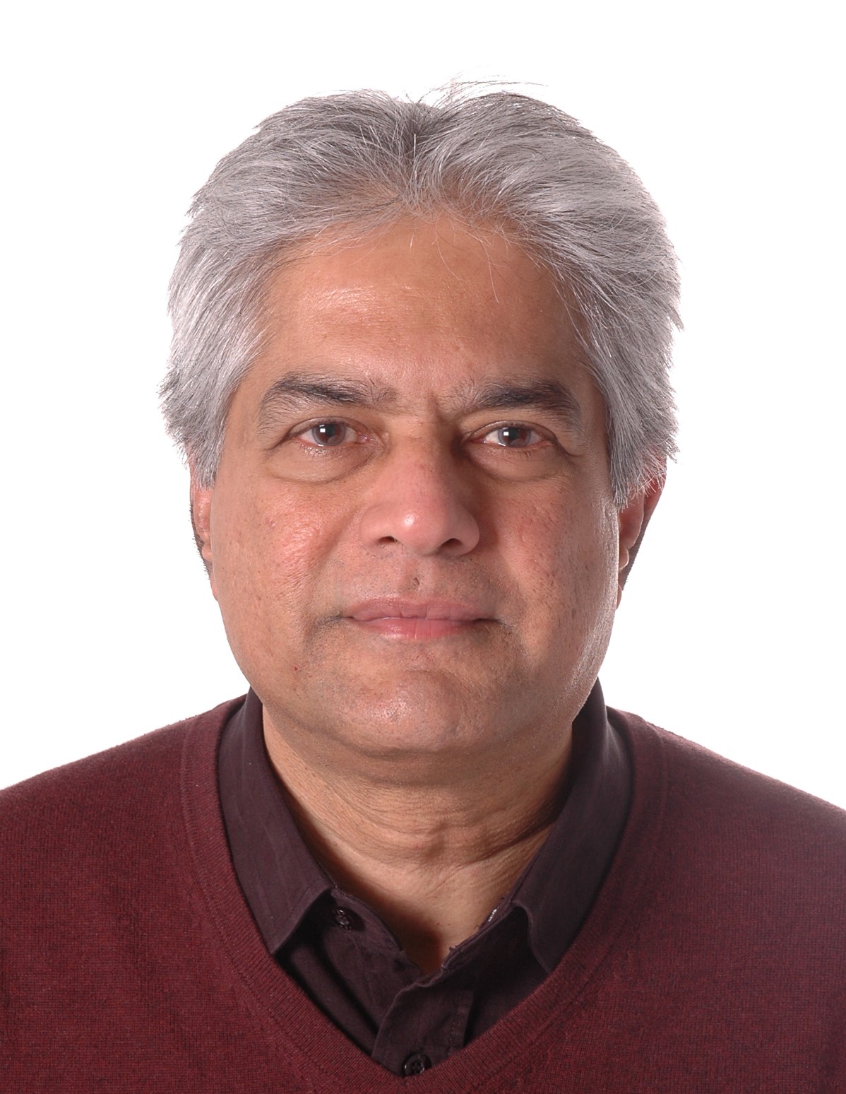
Arokia Nathan is currently a Bye-Fellow and Tutor at Darwin College, University of Cambridge, UK. He received his PhD degree in electrical engineering from the University of Alberta, Canada, in 1988. He joined LSI Logic USA, and subsequently, the Institute of Quantum Electronics, ETH Zürich, Switzerland, before joining the Electrical and Computer Engineering Department at the University of Waterloo, Canada. In 2006, he joined the London Centre for Nanotechnology, University College London, UK, as the Sumitomo Chair of Nanotechnology. He moved to Cambridge University in 2011 as the Chair of Photonic Systems and Displays. He has more than 600 publications, including six books, and more that 110 patents and four spin-off companies. He is the co-founder of Cambridge Touch Technologies, UK and VISBAN Networks UK where he is a Director and Chief Technical Officer. He is a Fellow of IEEE and SID, a Distinguished Lecturer of the IEEE Electron Devices Society and Sensor Council, a Chartered Engineer (UK), Fellow of the Institution of Engineering and Technology (UK), and winner of the 2020 IEEE EDS JJ Ebers Award.
Lecture Topics
- Flexible Electronics
- Oxide Semiconductor Electronics
- Ultralow Power Transistors and Sensor Interfaces
- Active Matrix OLED Displays
- TFT Compact Modeling and Parameter Extraction
- Nanoscale Large Area Electronics
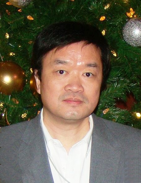
Ravi Todi received his M.S. degree in Electrical and Mechanical Engineering from University of Central Florida in 2004 and 2005 respectively, and his doctoral degree in Electrical Engineering in 2007. His graduate research work was focused on gate stack engineering, with emphasis on binary metal alloys as gate electrode and on high mobility Ge channel devices. In 2007 he started working as Advisory Engineer/Scientist at Semiconductor Research and Development Center at IBM Microelectronics Division focusing on high performance eDRAM integration on 45nm SOI logic platform. Starting in 2010 Ravi was appointed the lead Engineer for 22nm SOI eDRAM development. For his many contributions to the success of eDRAM program at IBM, Ravi was awarded IBM’s Outstanding Technical Achievement Award in 2011. Ravi Joined Qualcomm in 2012, responsible for 20nm technology and product development as part of Qualcomm’s foundry engineering team. Ravi is also responsible for early learning on 16/14 nm FinFet technology nodes. Ravi had authored or co-authored over 50 publications, has several issues US patents and over 25 pending disclosures.
Lecuture Topic
- MOS Devices and Technology
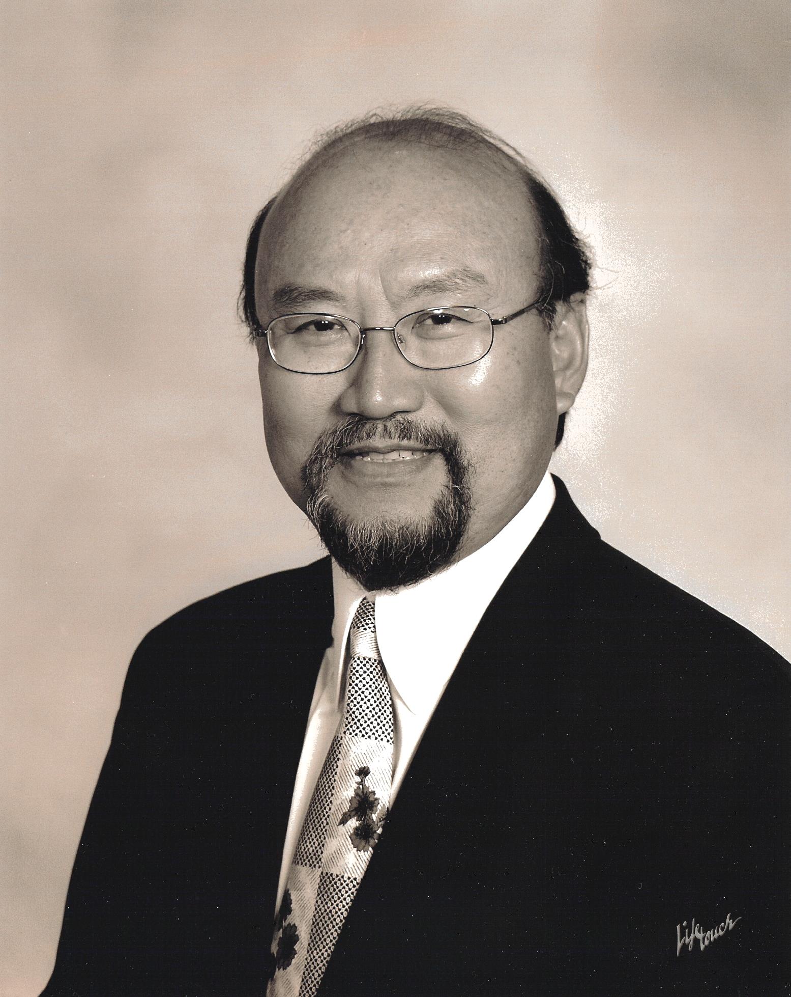
Cary Y. Yang received the B.S., M.S., and Ph.D. degrees in electrical engineering from the University of Pennsylvania. After working at M.I.T., NASA Ames Research Center, and Stanford University on electronic properties of nanostructure surfaces and interfaces, he founded Surface Analytic Research, a Silicon Valley company focusing on sponsored research projects covering various applications of surfaces and nanostructures. He joined Santa Clara University in 1983 and is currently Professor of Electrical Engineering and Director of TENT Laboratory, a SCU facility located inside NASA Ames. He was the Founding Director of Microelectronics Laboratory and Center for Nanostructures, and served as Chair of Electrical Engineering and Associate Dean of Engineering at Santa Clara. His research spans from silicon-based nanoelectronics to nanostructure interfaces in electronic, biological, and energy-storage systems. An IEEE Life Fellow, he served as Editor of the IEEE Transactions on Electron Devices, President of the IEEE Electron Devices Society, and elected member of the IEEE Board of Directors. He was appointed Vice Chair of the IEEE Awards Board in 2013 and 2014. He received the 2004 IEEE Educational Activities Board Meritorious Achievement Award in Continuing Education "for extensive and innovative contributions to the continuing education of working professionals in the field of micro/nanoelectronics," and the IEEE Electron Devices Society Distinguished Service Award in 2005. From 2008 to 2013, he held the Bao Yugang Chair Professorship at Zhejiang University in China.
Lecture Topics:
- Nanocarbon Interconnects
- CNT-graphene interface
Strategic Goals
1. Be the first place that students and technical professionals working in the field of electron devices go to for the information and services that are indispensable for their success.
2. Equitably foster diverse and inclusive communities of practice to facilitate information exchange, collaboration and professional development for greater technological innovation and excellence to benefit all humanity.
3. Establish a process and allocate sufficient resources to support innovative projects that apply electron devices and technology for humanity to address one or more of the United Nations sustainable development goals.
4. Develop synergistic relationships outside EDS to accelerate technological progress in multi-disciplinary areas.
Strategic Directions Committee Charter
Strategic Directions Webinars
Strategic Directions Webinar #1 Recording
Strategic Directions Webinar #2 Recording
Strategic Directions Webinar Slides
Member Feedback: https://ieee-collabratec.ieee.org/app/workspaces/8209/activities
The Future To Which We Aspire, by Doug Verret