- Home
- About EDS
- Governance
- Voting Forum
Voting Forum
As mentioned in the EDS Constitution, Section 1. There shall also be a Society Forum (Forum) consisting of all BoG members, Executive Committee members, and Standing and Technical Committee chairs all serving with voting privileges. In addition, all members serving on committees chaired by a voting member of the Forum shall be ex-officio members of the Forum without vote. Ad hoc committee chairs and chapter chairs shall also be ex-officio members of the Forum without vote.
Voting privileges: Voting on society administrative matters, but not on Elections or C&B changes
Officers
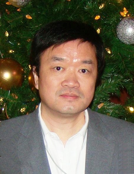
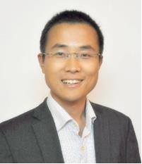
President
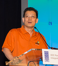
Bin Zhao - Fellow
Lecture Topics:
- Analog/Mixed-Signal/RF IC and Enabling Technologies
- High Performance VLSI Interconnect
President Elect
Arokia Nathan - Fellow
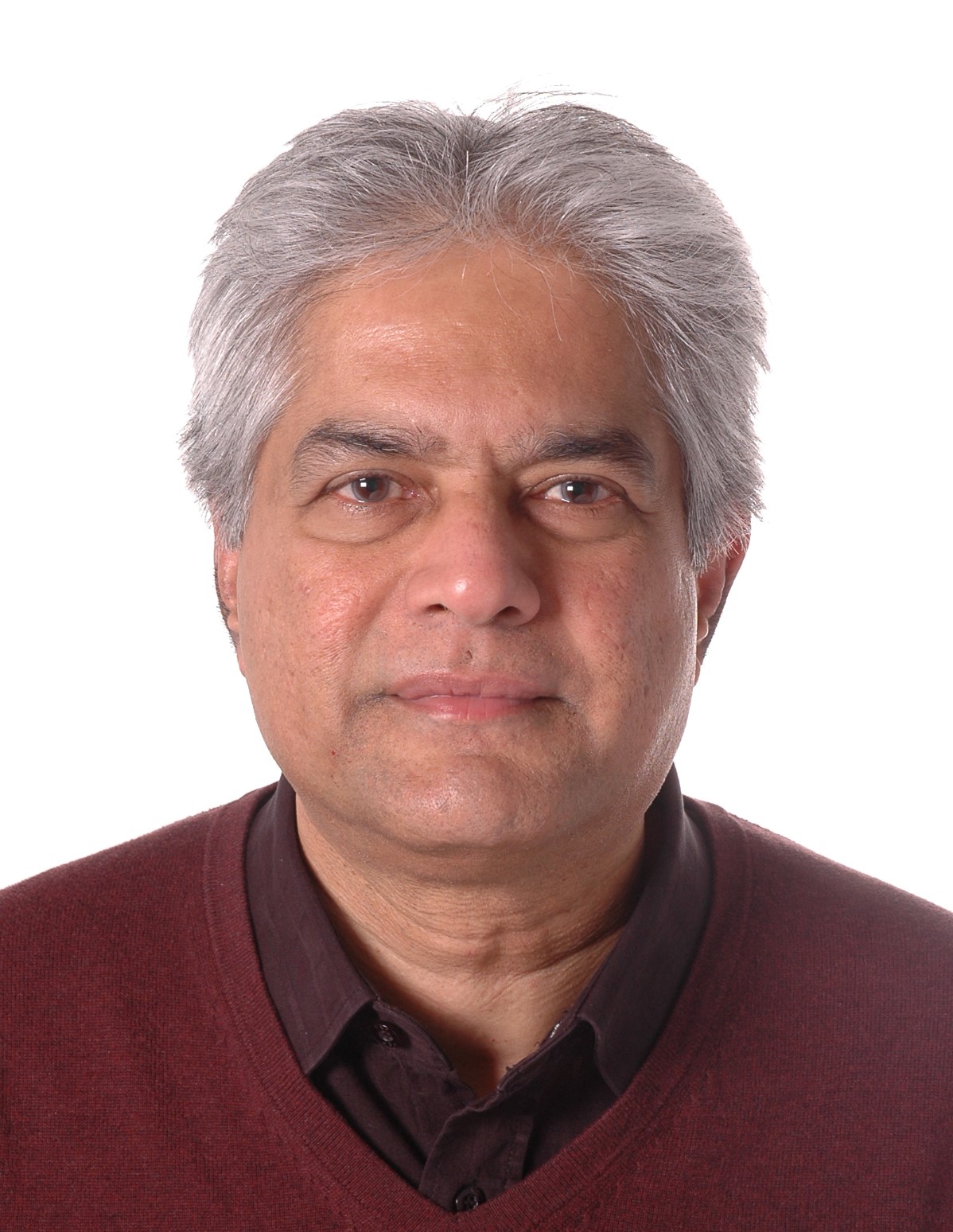
Arokia Nathan is currently a Bye-Fellow and Tutor at Darwin College, University of Cambridge, UK. He received his PhD degree in electrical engineering from the University of Alberta, Canada, in 1988. He joined LSI Logic USA, and subsequently, the Institute of Quantum Electronics, ETH Zürich, Switzerland, before joining the Electrical and Computer Engineering Department at the University of Waterloo, Canada. In 2006, he joined the London Centre for Nanotechnology, University College London, UK, as the Sumitomo Chair of Nanotechnology. He moved to Cambridge University in 2011 as the Chair of Photonic Systems and Displays. He has more than 600 publications, including six books, and more that 110 patents and four spin-off companies. He is the co-founder of Cambridge Touch Technologies, UK and VISBAN Networks UK where he is a Director and Chief Technical Officer. He is a Fellow of IEEE and SID, a Distinguished Lecturer of the IEEE Electron Devices Society and Sensor Council, a Chartered Engineer (UK), Fellow of the Institution of Engineering and Technology (UK), and winner of the 2020 IEEE EDS JJ Ebers Award.
Lecture Topics
- Flexible Electronics
- Oxide Semiconductor Electronics
- Ultralow Power Transistors and Sensor Interfaces
- Active Matrix OLED Displays
- TFT Compact Modeling and Parameter Extraction
- Nanoscale Large Area Electronics
Treasurer
Roger Booth

Secretary
Murty Polavarapu
Mail Stop MVA01-016
Jr. Past President
Ravi M. Todi
Ravi Todi received his M.S. degree in Electrical and Mechanical Engineering from University of Central Florida in 2004 and 2005 respectively, and his doctoral degree in Electrical Engineering in 2007. His graduate research work was focused on gate stack engineering, with emphasis on binary metal alloys as gate electrode and on high mobility Ge channel devices. In 2007 he started working as Advisory Engineer/Scientist at Semiconductor Research and Development Center at IBM Microelectronics Division focusing on high performance eDRAM integration on 45nm SOI logic platform. Starting in 2010 Ravi was appointed the lead Engineer for 22nm SOI eDRAM development. For his many contributions to the success of eDRAM program at IBM, Ravi was awarded IBM’s Outstanding Technical Achievement Award in 2011. Ravi Joined Qualcomm in 2012, responsible for 20nm technology and product development as part of Qualcomm’s foundry engineering team. Ravi is also responsible for early learning on 16/14 nm FinFet technology nodes. Ravi had authored or co-authored over 50 publications, has several issues US patents and over 25 pending disclosures.
Lecuture Topic
- MOS Devices and Technology
Elected Members
Elected Member Expiring 2024
Mario Aleman
Paul Berger - PV; mat for flexible electronics
Paul R. Berger
Ohio State University, Department of Electrical and Computer Engineering, Columbus, Ohio, USA
Tampere University, Department of Electronics and Communications Engineering, Printed and Organic Electronics Group, Tampere, Finland
Lecture Topics:
- Si-based Resonant Interband Tunnel Diodes for Quantum Functional and Multi-level Circuitry (Mixed-Signal, Logic, and Low Power Embedded Memory) to Extend CMOS
- Organic Photovoltaics: An Introduction to OPV plus Plasmonic enhancements (i.e. point-of-use energy harvesting, conformable to flexible and curved surfaces)
- Passive Millimeter Wave Imaging for Security and Safety via Si-based Backward Diode Sensors (i.e. detect concealed weapons and airplane safety for sight through fog, smoke and light rain)
- Fully Printed Flexible Internet-of-Things Nodes with Energy Scavenging and Non-toxic Energy Storage
- Nitride-Based Resonant Tunneling Structures for Terahertz Gain
- Unipolar-doped Co-Tunneling Structures: A new pathway for efficient light emission without P-type doping
- Solar-Powered Humanitarian Engineering: Tanzania, Colombia & USA
Paul R. Berger (S’84 M’91 SM’97 F’11) is a Professor in Electrical & Computer Engineering at Ohio State University and Physics (by Courtesy). He is also a Distinguished Visiting Professor at Tampere University in Finland. He received the B.S.E. in engineering physics, and the M.S.E. and Ph.D. (1990) in electrical engineering, respectively, all from the University of Michigan, Ann Arbor. Currently, Dr. Berger is actively working on quantum tunneling devices, printable semiconductor devices & circuits for IoT, bioelectronics, novel devices, novel semiconductors and applied physics.
Formerly, he worked at Bell Laboratories, Murray Hill, NJ (1990-’92) and taught at the University of Delaware in Electrical and Computer Engineering (1992-2000). In 1999, Prof. Berger took a sabbatical leave while working first at the Max-Planck Institute for Polymer Research, Mainz, Germany and then moved on to Cambridge Display Technology, Ltd., Cambridge, United Kingdom. In 2008, Prof. Berger spent an extended sabbatical leave at IMEC (Interuniversity Microelectronics Center) in Leuven, Belgium while appointed as a Visiting Professor in the Department of Metallurgy and Materials Engineering, Katholieke Universiteit Leuven, Belgium. Prof. Berger was also a Finnish Distinguished Professor (FiDiPro) at Tampere University of Technology (2014-2019), and he continues as a Fulbright-Nokia Distinguished Chair in Information and Communications Technologies (2020-2022) with the newly merged Tampere University.
He has authored over 240 referred publications and presentations with another ~100 plenary, keynote, invited talks, 5 book sections and been issued 25 patents with 3 more pending from 60+ disclosures with a Google Scholar H-index of 35. Some notable recognitions for Dr. Berger were an NSF CAREER Award (1996), a DARPA ULTRA Sustained Excellence Award (1998), Lumley Research Awards (2006, 2011), a Faculty Diversity Excellence Award (2009) and Outstanding Engineering Educator for State of Ohio (2014). He has been on the Program and Advisory Committees of numerous conferences, including the IEDM, DRC, ISDRS, EDTM and IFETC meetings. He will be hosting the IFETC in ’21 as General Chair. He currently is the Chair of the Columbus IEEE EDS/Photonics Chapter and Faculty Advisor to Ohio State’s IEEE Student Chapter. In addition, he is an elected member-at-large to the IEEE EDS Board of Governors (19’-21’), where he is also Vice Present of Strategic Directions (20’-21’) and a member of the EDS Finance Committee.
He is an IEEE EDS Fellow (2011) and Distinguished Lecturer (since 2011), as well as a Senior member of the Optical Society of America. He has received $9.9M in USA funding as lead PI, with an additional $26M as Co-PI in USA and €8.8M in funding through his Finnish partnerships. Altogether, he has received ~$47.5M in research funding.
Prof. Berger has established significant humanitarian engineering projects across the world with an emphasis on solar-power and sustainability. After completing a 6 year presence in Haiti to electrify remote schools with solar powered LED lighting as an Alternative Spring Break, Berger re-established two new international programs. (1) One through OSU’s Office of International Affairs, has traveled to Arusha, Tanzania with a group of engineering students from different majors to design, build and install a solar powered LED lighting system for an orphanage. (2) Additionally, through IEEE’s Humanitarian Activities Committee, Berger also proposed, and was funded, to provide solar-powered desalinization for the indigenous Wayúu peoples living in the Guajira peninsula desert. Also, the IEEE Electron Device Society has provided Berger additional funds to extend the Colombia project into 2020.
Yogesh Singh Chauhan - Device and Process Modeling
Department of Electrical Eng., Kanpur, India
Talk titles:
· Modeling and Simulation of Negative Capacitance Transistors
· Compact Modeling of GaN HEMTs using industry standard ASM-HEMT model
· Physics and Modeling of FinFET and Nanosheet Transistors
· Analog and RF Modeling in BSIM-BULK model
· Physics and Modeling of FDSOI Transistors
Yogesh Singh Chauhan is an associate professor at Indian Institute of Technology Kanpur (IITK), India. He was with Semiconductor Research & Development Center at IBM Bangalore during 2007 – 2010; Tokyo Institute of Technology in 2010; University of California Berkeley during 2010-2012; and ST Microelectronics during 2003-2004. He is the developer of several industry standard models: ASM-GaN-HEMT model, BSIM-BULK model (formerly BSIM6), BSIM-CMG model and BSIM-IMG model. His research group is involved in developing compact models for GaN transistors, FinFET, Nanosheet/Gate-All-Around FETs, FDSOI transistors, Negative Capacitance FETs and 2D FETs. His research interests are characterization, modeling, and simulation of semiconductor devices.
He is the Editor of IEEE Transactions on Electron Devices and Distinguished Lecturer of the IEEE Electron Devices Society. He is the member of IEEE-EDS Compact Modeling Committee and fellow of Indian National Young Academy of Science (INYAS). He is the founding chairperson of IEEE Electron Devices Society U.P. chapter and Vice-chairperson of IEEE U.P. section. He has published more than 200 papers in international journals and conferences.
He received Ramanujan fellowship in 2012, IBM faculty award in 2013 and P. K. Kelkar fellowship in 2015, CNR Rao faculty award, Humboldt fellowship and Swarnajayanti fellowship in 2018. He has served in the technical program committees of IEEE International Electron Devices Meeting (IEDM), IEEE International Conference on Simulation of Semiconductor Processes and Devices (SISPAD), IEEE European Solid-State Device Research Conference (ESSDERC), IEEE Electron Devices Technology and Manufacturing (EDTM), and IEEE International Conference on VLSI Design and International Conference on Embedded Systems.
Patrick Fay
Dept. of Electrical Engineering, IN, USA
Patrick Fay received a B.S. degree in Electrical Engineering from the University of Notre Dame in 1991, followed by the M.S. and Ph.D. degrees in Electrical Engineering from the University of Illinois at Urbana-Champaign in 1993 and 1996, respectively. He joined the faculty of the Department of Electrical Engineering at the University of Notre Dame in 1997, where he currently a professor as well as the director of the Notre Dame Nanofabrication Facility. His research interests include the design, fabrication, and characterization of III-V microwave and millimeter-wave electronic devices and circuits, power devices, and high-speed optoelectronic devices and optoelectronic integrated circuits. His research also includes the development and use of micromachining techniques for the fabrication of microwave and millimeter-wave components and packaging. Prof. Fay was awarded the Department of Electrical Engineering’s Outstanding Teacher award in 1998 and 2018, and Notre Dame's College of Engineering’s Outstanding Teacher award in 2015. He is a fellow of the IEEE, and Electron Device Society Distinguished Lecturer, and serves as an associate editor of the IEEE Transactions on Components, Packaging and Manufacturing Technology, IEEE Transactions on Electron Devices, and IEEE Transactions on Microwave Theory and Techniques.
Lecture Topics
- III-N Devices and Integration for Millimeter-Wave and Power Applications
- Vertical GaN Devices and Epitaxial Lift-Off Processing for High Performance Power Applications
- Advances in III-N Devices for Power and Internet of Things Applications
- III-N Nanowire FETs for Low-Power Applications
- Advanced Tunneling-Based Devices for mm-Wave Sensing and Imaging
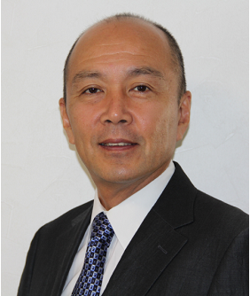
Kazunari Ishimaru
Bill Nehrer
Merlyne de Souza
Chair in Microelectronics, EEE Department
I graduated with a BSc in Physics and Mathematics (1985) from the University of Mumbai, a BE. in Electronics and Communications Engineering (1988) from the Indian Institute of Science, Bangalore and a PhD from the University of Cambridge (1994). I joined as a Junior Research fellow in ‘95, was promoted to a Senior Research fellow in ‘98 and was appointed Professor in Electronics and Materials at the Emerging Technologies Research Centre, De Montfort University in 2003. I joined the EEE department at Sheffield as Professor of Microelectronics in 2007. I work in multi-disciplinary research focused on the physics of devices, materials and their microelectronic applications in computing, communications and energy conversion.
Elected Member Expiring 2025
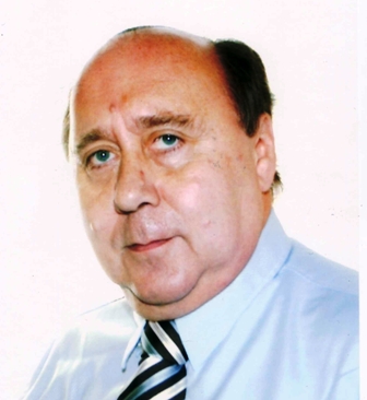
Constantin Bulucea - Distinguished Member of the Technical Staff
USA
Constantin Bulucea (S'69–M'70–SM'88–F'04- LF'13) was born in Râmnicu Vâlcea, Romania. In 1969, he got a one-year government scholarship at the University of California, Berkeley, where he received a M.S. degree in Electrical Engineering. In 1974, he received his Doctor degree in Electronics from the Polytechnic Institute of Bucharest with a thesis on hot-carrier injection in silicon. His original results were communicated at IEDM and published in the old (W. Crawford Dunlap’s) Solid-State Electronics. In Romania, he created the Annual Conference on Semiconductors, now an international IEEE event. His best known contribution from that period is the explanation of Grove’s breakdown voltage collapse in silicon gate-controlled devices as a breakdown-location switching phenomenon, as proven by 2-D computer calculations and measurements. Among his “firsts” from the same time is the direct proof, by DC recordings (rather than by capacitive inferences) of nA-range hot-carrier currents through silicon dioxide.
In 1886, Dr. Bulucea defected to the US, where he first developed a device/process architecture for rugged trench power DMOS transistors, while working for Siliconix (1987-1989). His inventive design became a world standard in the following years. Later on, at National Semiconductor (NS), he was a member of the Fairchild Research Center, then joined the company’s process development group. There, he enjoyed the last years of Silicon Valley's "Happy Scaling" as the architect of several CMOS processes for high-performance analog and mixed-signal applications (2000-2010). In 2011, he became a Distinguished Member of the Technical Staff of Texas Instruments (TI), as a result of TI's acquisition of NSC. Throughout his tenure at NS and TI, he received three Patent of the Year awards, in recognition of the use of his inventions in high-volume manufacturing. He has published over 50 technical articles in major journals and has 70 issued US patents. In 2001, he was elected an Honorary Member of the Romanian Academy and in 2004 became an IEEE Fellow "for contributions to transistor engineering in the area of power electronics".
Dr. Bulucea has been a member of the Technical Committees of the Bipolar Circuits and Technology Meeting (BCTM) and of the VLSI Technology Symposium. Between 2004 and 2012 he was the editor of IEEE Electron Device Letters (EDL) for analog and mixed-signals technology. His IEEE responsibilities include membership in the IEEE/EDS Fellow Evaluation Committee (2018, 2019) and the IEEE/EDS Publications Committee (current).
Daniel Mauricio Camacho Montejo
Folsom Design Center
John Dallesasse
University of Illinois at Urbana-Champaign
John Dallesasse is a Professor of Electrical and Computer Engineering and Associate Dean in the Grainger College of Engineering at the University of Illinois at Urbana-Champaign, where he’s been for over 10 years. He also has over 20 years of industry experience in technology development and executive management, having led technically diverse and geographically distributed engineering teams. Prior to joining UIUC he was the Chief Technology Officer, Vice President, and co-founder of Skorpios Technologies where he was responsible for developing innovative methods for heterogeneous integration of compound semiconductors with silicon. His technical contributions include, with Nick Holonyak, Jr., the discovery of III‑V Oxidation, which has become an enabling process technology for the fabrication of Vertical-Cavity Surface-Emitting Lasers (VCSELs) for optical networking, 3D imaging, and LIDAR applications. John has over 100 publications and conference presentations, and 50 issued patents. He serves as the Chair of the Steering Committee for the IEEE Journal of Lightwave Technology, the Chair of the Steering Committee for the IEEE Transactions on Semiconductor Manufacturing, and as the Vice President of Technical Committees for IEEE-EDS. He is a Fellow of the IEEE and Optica.
Mario Lanza - Senior Member
Mario Lanza is an Associate Professor of Materials Science and Engineering at the King Abdullah University of Science and Technology (KAUST), in Saudi Arabia since October 2020. Dr. Lanza got his PhD in Electronic Engineering with honors in 2010 at Universitat Autonoma de Barcelona. During the PhD he was a visiting scholar at The University of Manchester (UK) and Infineon Technologies (Germany). In 2010-2011 he was NSFC postdoc at Peking University, and in 2012-2013 he was Marie Curie postdoc at Stanford University. On October 2013 he joined Soochow University as Associate Professor, and in March 2017 he was promoted to Full Professor. Prof. Lanza has published over 120 research papers, including Science, Nature Electronics, Nature Chemistry, and IEDM, edited a book for Wiley-VCH, and registered four patents (one of them granted with 5.6 Million CNY). Prof. Lanza has received the 2017 Young Investigator Award from Microelectronic Engineering (Elsevier), and the 2015 Young 1000 Talent award (among others), and in 2019 he was appointed as Distinguished Lecturer of the Electron Devices Society (IEEE-EDS). Prof. Lanza is Associate Editor of Scientific Reports (Nature) and Microelectronic Engineering (Elsevier), and serves in the board of many others, like Advanced Electronic Materials (Wiley-VCH), Nanotechnology and Nano Futures (IOP). He is also an active member of the technical committee of several world-class international conferences, including IEEE-IEDM, IEEE-IRPS, IEEE-IPFA and APS. Prof. Lanza leads a research group formed by 10-15 PhD students and postdocs, and they investigate how to improve electronic devices using 2D materials, with special emphasis on two-dimensional (layered) dielectrics and memristors for non-volatile digital information storage and artificial intelligence computing systems.
Lecture title:
- Two-dimensional materials based electronic devices
Lluis F. Marsal - Senior Member
Prof. Lluis F. Marsal is Distinguished Professor and full professor at the University Rovira i Virgili, Spain. Ph.D. from the University Politecnica de Catalunya, Spain, 1997. Postdoctoral researcher at the ECE, University of Waterloo, Canada (1998-1999). In 2014, he received the UniSA Distinguished Researcher Award, and the 2014 ICREA Academia Award from the Generalitat of Catalunya. Since 2019, he is the Chair of the Subcommittee for Regions/Chapters (SRC) Regions 8, IEEE- EDS. He was the Chair of Spain Chapter of the IEEE-EDS (2013-2018). He is a senior member of the IEEE and a member of the Distinguished Lecturer program of the EDS. He has co-authored more than 200 publications in international refereed journals, 2 books, 5 book chapters and 3 patents. His current research interests focus on organic solar cells and hybrid nanostructured materials for optoelectronic devices and low-cost technologies based on micro- and nanoporous materials for biosensing. Lecture Topics: Current progress and perspectives in polymer solar cells Nanostructured organic solar cells and polymers for flexible optoelectronic applications Photonic and optoelectronic devices based on porous materials Micro- and nanoporous materials for biosensing
Lecture Topics:
-Organic photovoltaic solar cells
-Nanostructured polymers and porous materials
-Photonic and optoelectronic devices
-Optical Biosensors
Geok Ing Ng - Compound Devices and RF Applications
Mayank Shrivastava - Compound Semiconductor Devices
India
Biography: Prof. Mayank Shrivastava is a faculty member at the Indian Institute of Science, Bangalore, and co-founder of AGNIT Semiconductors Pvt. Ltd. He is also instrumental in setting up a 300 Crore worth GaN prototyping Fab and leading a national effort on 2D material’s technology hub. He received his Ph.D. degree from the Indian Institute of Technology Bombay (2010). For his Ph.D. work, he received Excellence in Research award and the Industrial Impact award from IIT Bombay in 2010. He is among the first recipients of the Indian section of the American TR35 award (2010) and the first Indian to receive IEEE EDS Early Career Award (2015). He is also an Editor of IEEE Transactions on Electron Devices. Besides, he is an IEEE Electron Device’s Society (EDS) Distinguished Lecturer and an elected member of the IEEE EDS Board of Governors. He is the recipient of the prestigious DST Swarnjayanti Fellowship (2021), Abdul Kalam Technology Innovation National Fellowship from INAE-SERB (2021), and the VASVIK award (2021). He has received several other national awards and honors of high repute, like the National Academy of Sciences, India, (NASI) Young Scientist Platinum Jubilee Award – 2018; Indian National Academy of Science (INSA) Young Scientist Award - 2018; Indian National Academy of Engineering (INAE) Innovator Entrepreneur Award 2018 (Special commendation); Indian National Academy of Engineering (INAE) Young Engineer Award - 2017; INAE Young Associate (since 2017); Indian Academy of Sciences (IASc), Young Associate, 2018 – 2023; Ministry of Electronics & Information Technology (MeitY), Young Faculty Fellowship. Besides, he received best paper awards from several international conferences like Intel Corporation Asia academic forum, VLSI design Conference and EOSESD Symposium. Prof Shrivastava broadly works on applications of emerging materials like Gallium Nitride (GaN), atomically thin two-dimensional materials like Graphene and TMDCs, in electronic and electro-optic devices working closer to its fundamental limits (like the ability to handle extreme powers, ability to work at THz like ultra-high frequencies, or ability to compute information in unconventional ways). Currently, his group is developing few-atom thick devices & circuits, GaN-based ultra-high-power devices with high reliability, and devices/circuits for operation at THz frequencies. Besides, his group also works on developing novel ESD and High Voltage device concepts in advanced CMOS nodes. He held visiting positions in Infineon Technologies, Munich, Germany, from April 2008 to October 2008 and again from May 2010 to July 2010. He worked for Infineon Technologies, East Fishkill, NY, USA; IBM Microelectronics, Burlington, VT, USA; Intel Mobile Communications, Hopewell Junction, NY, USA; Intel Corp, Mobile and Communications Group, Munich, Germany between 2010 and 2013. He joined the Indian Institute of Science as a faculty member in the year 2013. Prof Shrivastava’s work has resulted in over 200 peer-reviewed publications (47 of these papers are in IRPS and IEDM, the two most prestigious conferences of IEEE EDS, and around 100 are in journals such as IEEE T-ED) and 47 patents. Most of these patents are either licensed by semiconductor companies or are in use in their products. More details are available at https://faculty.dese.iisc.ac.
Elected Member Expiring 2026
Harshit Agarwal
Xiaojun Guo - Optoelectronics, Display, Imaging
Xiaojun Guo is now Professor in Department of Electronic Engineering at Shanghai Jiao Tong University, China. He received the Bachelor degree from Jilin University (China) in 2002, and the Ph.D. degree from University of Surrey (UK) in 2007, both in electronic engineering. He worked on EDA for VLSIs in Department of Electronic Engineering at Tsinghua University during 2002-2003. His PhD research was on system-on-panel integration with low-temperature poly-Si TFTs. Before joining Shanghai Jiao Tong University in Aug. 2009, he had been working in Plastic Logic Ltd., Cambridge, UK, on research and development of printed polymer TFTs backplanes for flexible displays, and technology transfer for manufacturing. His group at Shanghai Jiao Tong University is now focusing on device and integration of printable thin film transistors and functional devices including displays, sensors and memories. He has authored or co-authored more than 60 technical papers in international journals and conference.
Lecture Titles
-Thin-fi lm transistor for Flexible Heterogeneous Integration
-Organic thin-fi lm Transistor for Display and Sensor Integration
-Low power Flexible Hybrid Integration for IoT
-Active-Matrix Backplane Design and Integration for Advanced Displays
Francesca Iacopi
School of Electrical and Data Engineering | Faculty of Engineering & IT
Professor Francesca Iacopi is an IEEE Fellow with over 20 years’ industrial and academic research expertise in semiconductor technologies, with 160 peer-reviewed publications and 10 granted US patents, spanning interconnects, CMOS devices and packaging. Her research focuses on the translation of basic scientific advances in nanomaterials and novel device concepts into implementable integrated technologies. She is known for her seminal work on the integration of porous dielectrics in on-chip interconnects, and for the invention of the alloy -mediated epitaxial graphene platform on SiC/Si pseudo-substrates. She was recipient of an MRS Gold Graduate Student Award (2003), an Australian Research Council Future Fellowship (2012), a Global Innovation Award in Washington DC (2014) and was listed among the most innovative engineers by Engineers Australia (2018). Francesca is an IEEE EDS Distinguished Lecturer and serves regularly in technical and strategic committees for IEEE and the Materials Research Society. She is an Elected Member to the IEEE EDS Board of Governors (2021, 2024) and serves in the Editorial Advisory Board for ACS Applied Nanomaterials, and the IEEE The Institute magazine. She is also the inaugural Editor-in-Chief of the IEEE Trans. on Materials for Electron Devices (IEEE T-MAT). She leads the Integrated Nanosystems Lab, in the Faculty of Engineering and IT, University of Technology Sydney. She is a Chief Investigator of the CoE in Transformative Meta-Optical Systems (TMOS), funded by the Australian Research Council.
Meikei Ieong - Fellow
Chief Technology Officer
Biography: Meikei Ieong (SM’01) received the B.S. degree in electrical engineering from the National Taiwan University, Taipei, Taiwan, in 1991 and the M.S. and Ph.D. degrees in electrical and computer engineering from the University of Massachusetts, Amherst, in 1993 and 1996, respectively. He also received an MBA degree from the Sloan Fellows Program of Massachusetts Institute of Technology in 2013.
Meikei is currently Vice-President of TSMC Europe. He was program director of TSMC’s 28nm High-Performance and Mobile Technologies. Prior to that he held various engineering and management positions at IBM including senior manager at IBM TJ. Watson Research Center, Yorktown, NY. He’s recipient of IBM Technical Achievement and Corporate awards and was elected as a Master Inventor at IBM Research.
He held an adjunct associate professor position with the Department of Electrical Engineering from the Columbia University, NY in 2001. He was General Chairman of the IEEE International Electron Devices Meeting (IEDM). He has served as an editor for the IEEE Transaction on Electron Devices since 2010 and as chair of the IEEE EDS Education Award committee since 2013. He has Published more than one hundred papers in referred journals and conference proceedings and more than eighty patents. He also speaks frequently at international conferences and seminars.
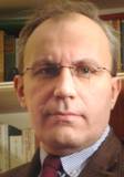
Andreas Kerber
Andreas Kerber was born in Schnann, Austria. He received his Diploma in physics from the University of Innsbruck, Austria, in 2001 and a PhD in electrical engineering from the TU-Darmstadt, Germany in 2004 (granted with honors). He worked as an intern at Bell Laboratories, Lucent Technologies, Murray Hill, NJ, USA (1999-2000), at IMEC in Leuven, Belgium (2001-03) as Infineon Technologies assignee to International SEMATECH, for the Reliability Methodology Department at Infineon Technologies in Munich, Germany (2004-06), for AMD in Yorktown Heights, NY (2006-09), and as a Prinicpal Member of Technical Staff for GLOBALFOUNDRIES in Malta, NY (since 2009). Much of his work centered around Front-End-Of-Line (FEOL) reliability research with focus on metal gate / high-k CMOS technologies. He has co-authored over 100 papers in Journals and Conferences, is an IEEE senior member (since 2011) and an IEEE Distinguished Lecturer for the Electron Device Society (since 2016).
Lecture Topics
Reliability of scaled Metal Gate / High-K CMOS devices
P Susthitha Menon - Optoelectronics, Photonics
National University of Malaysia (UKM)
P Susthitha Menon is currently an Associate Professor at the Universiti Kebangsaan Malaysia (UKM) at Kuala Lumpur. She received her BSEE degree from (UKM) in 1998. As an Intel scholar, she worked at Intel Malaysia as a Product Engineer for mobile modules systems from 1999 to 2002. She then received her MSc and PhD (Distinction) degrees in 2005 and 2008 respectively from UKM, for the development of Si- and InGaAs-based interdigitated p-i-n photodiodes. At the University’s Institute of Micro-Engineering & Nanoelectronics (IMEN) she is specializing in the field of optoelectronics, nanophotonics, and robust engineering optimization. Susthitha is a Senior Member of IEEE. She is in the organizing team international conference ICSE by ED Malaysia Chapter for many years and is the Secretary of the IEEE Electron Devices Malaysia Chapter.
Luisa Petti
Camilo Velez Cuervo
Standing Committees
Awards Committee Chair
Ravi M. Todi
Ravi Todi received his M.S. degree in Electrical and Mechanical Engineering from University of Central Florida in 2004 and 2005 respectively, and his doctoral degree in Electrical Engineering in 2007. His graduate research work was focused on gate stack engineering, with emphasis on binary metal alloys as gate electrode and on high mobility Ge channel devices. In 2007 he started working as Advisory Engineer/Scientist at Semiconductor Research and Development Center at IBM Microelectronics Division focusing on high performance eDRAM integration on 45nm SOI logic platform. Starting in 2010 Ravi was appointed the lead Engineer for 22nm SOI eDRAM development. For his many contributions to the success of eDRAM program at IBM, Ravi was awarded IBM’s Outstanding Technical Achievement Award in 2011. Ravi Joined Qualcomm in 2012, responsible for 20nm technology and product development as part of Qualcomm’s foundry engineering team. Ravi is also responsible for early learning on 16/14 nm FinFet technology nodes. Ravi had authored or co-authored over 50 publications, has several issues US patents and over 25 pending disclosures.
Lecuture Topic
- MOS Devices and Technology
Communications Committee Chair
Bernard Lim
Vice President of Educational Activities
Mansun J. Chan - Fellow
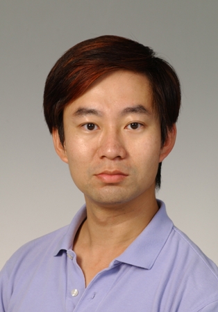
Lecture Topics:
- Nano-device physics and technology
- Device modelling and circuit simulation
- Interconnect Technology
- Non-volatile memory technology
- Bio-sensors and circuits
Biography: Mansun Chan (S’92-M’95-SM’01-F’13) received Ph.D. degrees from the UC, Berkeley in 1995. He is one of the major contributors to the unified BSIM model for SPICE, which has been accepted by most US companies and the Compact Model Council (CMC) as the first industrial standard MOSFET model. In January 1996, he has joined the EEE faculty at Hong Kong University of Science and Technology. After that, he developed a SOI MOSFET model, which has been adopted by UC Berkeley as the core of the BSIMSOI model. Between July 2001 and December 2002, he was a Visiting Professor at University of California at Berkeley and the Co-director of the BSIM program. In this capacity, he has successfully completed the technology transfer of BSIM3SOI to be the first industrial standard SOI MOSFET model. In addition to device modeling, Prof. Chan’s current research interests also include nano-transistor fabrication technology, carbon-based device physics, printable transistors, 3D integrated circuits, bio-sensors and cloud computing based simulation platform. He is current working on an interactive modeling and online simulation (i-MOS) platform to facilitate the interactions between model developers and circuit designers using the Internet technology.
Prof. Chan is a recipient of the UC Regents Fellowship, Golden Keys Scholarship for Academic Excellence, SRC Inventor Recognition Award, Rockwell Research Fellowship, R&D 100 award (for the BSIM3v3 project), Teaching Excellence Appreciation award, Distinguished Teaching Award and the Shenzhen City Technology Innovation Award by the Chinese Government. He is a Fellow and Distinguished Lecturer of IEEE.
Fellow Evaluation Committee Chair
Albert Z.H. Wang - Fellow - IEEE
Dept. of Electrical and Computer Engineering
Albert Wang is a Professor of Electrical and Computer Engineering at the University of California, Riverside, USA. His research interests cover semiconductor devices, AMS/RF ICs, integrated design-for-reliability, 3D heterogeneous devices and integration, emerging nano devices and circuits. He authored 2 book and more than 320 papers, and holds 16 US patents. He was President for IEEE Electron Devices Society (2014-2015). He is/was editor for seven IEEE journals. He has been an IEEE Distinguished Lecturer for IEEE Electron Devices Society, IEEE Solid-State Circuits Society and IEEE Circuits and Systems Society. His other services include ITRS committee, IEEE 5G Initiative committee, IEEE HIR committee, IEEE Fellow Committee, and chair for IEEE CAS ASPTC and IEEE EDS Fellow committee. He was General Chair (2016) for IEEE RFIC Symposium and is General Chair (2021) for IEEE EDTM conference. He was Program Director of National Science Foundation, USA. He is recipient of IEEE EDS J. J. Ebers Award and IEEE EDS Distinguished Service Award. He is Fellow of National Academy of Inventors, Fellow of IEEE and Fellow of AAAS..
Finance Committee Chair
Roger Booth
Humanitarian Committee Chair
Cor L. Claeys - Fellow
Cor Claeys is Professor at the KU Leuven (Belgium) since 1990. He was with imec, Leuven, Belgium from 1984 till 2016. His main interests are semiconductor technology, device physics, low frequency noise phenomena, radiation effects and defect engineering. He co-edited books on “Low Temperature Electronics” and “Germanium-Based Technologies: From Materials to Devices” and wrote monographs on “Radiation Effects in Advanced Semiconductor Materials and Devices”, “Fundamental and Technological Aspects of Extended Defects in Germanium” and “Random Telegraph Signals in Semiconductor Devices” and “Metals in Silicon- and Germanium-Based Technologies: Origin, Characterization, Control and Electrical Impact”. He (co)authored 14 book chapters, over 1100 conference presentations and more than 1300 technical papers. He is editor/co-editor of 60 Conference Proceedings. Prof. Claeys is a Fellow of the Electrochemical Society and of IEEE. He was Founder of the IEEE Electron Devices Benelux Chapter, Chair of the IEEE Benelux Section, elected Board of Governors Member and EDS Vice President for Chapters and Regions. He was EDS President in 2008-2009 and Division Director on the IEEE Board of Directors in 2012-2013. He is a recipient of the IEEE Third Millennium Medal and received the IEEE EDS Distinguished Service Award. Within the Electrochemical Society, he was Chair of the Electronics & Photonics Division (2001-2003) . In 2004, he received the Electronics & Photonics Division Award.
Lecture Topics:
* Low Frequency Noise in state of the art and emerging semiconductor technologies
* Radiation Hardness of State-of-the-art Si and Ge-Based CMOS Technologies
* Are Extended Defects a Show Stopper for Future III-V CMOS Technologies?
* Trends and Challenges in Micro- and Nanoelectronics for the Next Decade
Vice President of Meetings and Conferences
Shuji Ikeda
NIRC
Shuji Ikeda (M’91-SM’02-F’04) received the B.S. degree in Physics, PhD. in Electrical Engineering from Tokyo Institute of Technology, Tokyo, Japan in 1978 and 2003 respectively and the M.S. degree in Electrical Engineering from Princeton University, Princeton, New Jersey, USA in 1987. He joined Semiconductor and Integrated Circuit Group, Hitachi ltd., Tokyo, Japan in 1978, where he was engaged in research and development of state of the art SRAM process and devices. He was also working on developing process technology for LOGIC, embedded memories, and CMOS power RF devices and on transferring technology to mass production line. He invented some of the outstanding structures for SRAM. He pioneered process to implement new materials in mass production, including W-polycide, Al-Cu-Si in 1984 and in-situ phosphorus-doped-polysilicon in 1990. He is the first to realize Lightly Doped Drain (LDD) in production to suppress Hot Carrier Injection in 1984. He also firstly implemented polyimide coat of the chip to immune SER caused by alpha particle from the resin covers the chip. In October 2000, he joined Trecenti Technologies Inc. He developed new process scheme with aggressive reduction of process time and suitable for single-wafer processing. That achieved less than 0.25days/layer cycle time. In April 2005, he joined ATDF at Austin Texas, as a Director of Technology. Where he develops various kinds of technologies includes scaled CMOS, non-classical CMOS, new materials and tools. He established tei Technology LLC in May 2008, Omni Water Solutions LLC, in 2009 at Austin Texas. He started tei Solutions Inc in Tsukuba, Ibaraki, Japan in 2010, where, he manages R&D foundry developing new devices, process technologies for VLSIs. He also integrates emerging technology onto semiconductor manufacturing technology to create innovative products/businesses. Due to his contributions to 200 MHz RISC microprocessor, he got 1999 R&D 100 Award. He served as subcommittee and executive committee member of IEDM from 1993 to 2002. He introduced Manufacturing Session in 1998 and chaired IEDM in 2002. He was a member of EDS Administrative Committee from 2005 to 2010. He was a technical program member for VLSI Technology Symposium in 2007 and 2008. He serves as a chairman of VLSI committee of EDS from 2009 and AdHoc Committee on Asia EDS Conference from 2014.
Vice President of Membership and Services
Durga Misra - Senior Member
- Nanoelectronics to Nanotechnology: More Moore and More than Moore
- Self-Heating in FinFETs and Its Impact on Logic Circuits
Newsletter Oversight Committee Chair
Murty Polavarapu
Mail Stop MVA01-016
Nominations & Elections Committee Chair
Ravi M. Todi
Ravi Todi received his M.S. degree in Electrical and Mechanical Engineering from University of Central Florida in 2004 and 2005 respectively, and his doctoral degree in Electrical Engineering in 2007. His graduate research work was focused on gate stack engineering, with emphasis on binary metal alloys as gate electrode and on high mobility Ge channel devices. In 2007 he started working as Advisory Engineer/Scientist at Semiconductor Research and Development Center at IBM Microelectronics Division focusing on high performance eDRAM integration on 45nm SOI logic platform. Starting in 2010 Ravi was appointed the lead Engineer for 22nm SOI eDRAM development. For his many contributions to the success of eDRAM program at IBM, Ravi was awarded IBM’s Outstanding Technical Achievement Award in 2011. Ravi Joined Qualcomm in 2012, responsible for 20nm technology and product development as part of Qualcomm’s foundry engineering team. Ravi is also responsible for early learning on 16/14 nm FinFet technology nodes. Ravi had authored or co-authored over 50 publications, has several issues US patents and over 25 pending disclosures.
Lecuture Topic
- MOS Devices and Technology
Vice President of Publications and Products
Giovanni Ghione - Editor-in-Chief
Department of Electronics and Telecommunications, Torino, Italy
Giovanni Ghione graduated cum laude in Electronic Engineering from Politecnico di Torino, Torino Italy in 1981. He was Assistant Professor in Electromagnetic Fields since 1983, Associate Professor in Circuit Theory with Politecnico di Milano, Milano Italy since 1987, and finally Full Professor in Electronics since 1990, first with University of Catania, then again with Politecnico di Torino. His research activity has been mainly concerned with high-frequency electronics and optoelectronics. He has contributed to the physics-based modelling of compound semiconductor devices, with particular interest in the numerical noise modeling in the small- and large-signal regimes, in the thermal modeling of devices and integrated circuits, and in the modeling of widegap semiconductors devices and materials. He has also done research in the field of microwave electronics, with contributions in the modeling of passive elements, in particular coplanar components, and in the design of power MMICs. Prof. Ghione was actively engaged since 1985 in research on optoelectronic devices, with application to the modeling and design of near and far-IR photodetectors, electrooptic and electroabsorption modulators, and GAN-based LEDs. Prof. Ghione has authored or co-authored more than 300 research papers on the above subjects and five books. He is an IEEE Fellow (class 2007). He has been a member of the QPC subcommitee of IEDM in 1997-1998 and in 2006-2007 and Chair in 2008; in 2009-2010 he was the EU Arrangement Co-Chair of IEDM. From 2010 to 2015 he has been chair of the EDS Committee on Compound Semiconductor Devices and Circuits. He has been Chair of the GAAS2003 conference and he has been subcommittee chair in several SCs of the European Microwave Week. He was President of the Library System of Politecnico from 1997 to 2007. From 2007 to 2015 he was the Head of the Department of Electronics and Telecommunications of Politecnico di Torino.
Vice President of Regions and Chapters
Benjamin Iniguez - Senior Member
Benjamin Iñiguez obtained the Ph D in Physics in 1992 and 1996, respectively, from the Universitat de les Illes Balears (UIB). From February 1997 to September 1998 he was working as a Postdoctoral Researcher at the Rensselaer Polytecnhnic Institute in Troy (NY, USA). From September 1998 to January 2001 he was working as a Postdoctoral Scientist in the Université catholique de Louvain (Louvain-la-Neuve, Belgium), supported by two Marie Curie Fellowships from the European Commission. In February 2001 he joined the Department of Electronic, Electrical and Automatic Control Engineering (DEEEiA)of the Universitat Rovira i Virgili (URV), in Tarragona, Catalonia, Spain) as Titular Professor. In February 2010 he became Full Professor at URV. He obtained the Distinction from the Generalitat for the Promotion of University Research in 2004 and the ICREA Academia Award (the highest award for university professors in Catalonia, from ICREA Institute) in 2009 and 2014, for a period of 5 years each. He led one EU-funded project (“COMON”, 2008-12) devoted to the compact modeling of nanoscale semiconductor devices and he is currently leading one new EU-funded project (DOMINO, 2014-18) targeting the compact modeling of organic and oxide TFTs. His main research interests are the characterization, parameter extraction and compact modelling of emerging semiconductor devices, in particularorganic and oxide Thin-Film Transistors, nanoscale Multi-Gate MOSFETs and GaN HEMTs. He has published more than 150 research papers in international journals and more than 130 abstracts in proceedings of conferences.
Lecture Topics
Compact device modeling
Semiconductor device parameter extraction
Physics of Thin-Film Transistors
Graphene and TMD devices
Vice President of Strategic Directions
John Dallesasse
University of Illinois at Urbana-Champaign
John Dallesasse is a Professor of Electrical and Computer Engineering and Associate Dean in the Grainger College of Engineering at the University of Illinois at Urbana-Champaign, where he’s been for over 10 years. He also has over 20 years of industry experience in technology development and executive management, having led technically diverse and geographically distributed engineering teams. Prior to joining UIUC he was the Chief Technology Officer, Vice President, and co-founder of Skorpios Technologies where he was responsible for developing innovative methods for heterogeneous integration of compound semiconductors with silicon. His technical contributions include, with Nick Holonyak, Jr., the discovery of III‑V Oxidation, which has become an enabling process technology for the fabrication of Vertical-Cavity Surface-Emitting Lasers (VCSELs) for optical networking, 3D imaging, and LIDAR applications. John has over 100 publications and conference presentations, and 50 issued patents. He serves as the Chair of the Steering Committee for the IEEE Journal of Lightwave Technology, the Chair of the Steering Committee for the IEEE Transactions on Semiconductor Manufacturing, and as the Vice President of Technical Committees for IEEE-EDS. He is a Fellow of the IEEE and Optica.
Technical Committees
Vice President Technical Activities (Interdisciplinary)
Chen Yang - Sensors and Actuators
Wilmington, MA
Chen Yang received his B. S. degree and Ph.D. degree in Electronic Science and Technology from Tsinghua University, Beijing, China, in 2003 and 2008, respectively. He was a Postdoctoral Researcher at University of California at Berkeley from 2009 to 2010. Then he joined Shanghai Institute of Microsystem and Information Technology, Chinese Academy of Sciences, as an Associate Professor. From 2013 to 2016, he worked as an Assistant Project Scientist at the Berkeley Sensors and Actuators Center (BSAC), University of California at Berkeley. Since 2016, he is with Analog Devices, Inc. in advanced MEMS development team. His research interests include MEMS physical and biological sensors, energy storage devices, RF passive devices and nano-materials. Dr. Yang was the recipients of the IEEE Electron Devices Society (EDS) Early Career Award in 2010, and the IEEE ElectronDevices Society Ph.D. Student Fellowship Award in 2007. He has been serving as TPC member of IEEE RFIC Symposium since 2012. He served as the vice chair of IEEE EDS Regions 4-6 SRC and member of the EDS Membership Committee. He was the tutorial chair of 2009 Silver Jubilee Conference on Communication Technologies and VLSI Design (CommV) at Vellore, Tamil Nadu, India, the secretary of the 3rd Japan-China-Korea Joint Conference on MEMS/NEMS (JCK MEMS/NEMS 2012) at Shanghai, China, and the secretary of 2007 International Workshop on Electron Devices and Semiconductor Technology (IEDST 2007) at Beijing, China. He was the founding Chair of IEEE Electron Devices Society Tsinghua University Student Branch Chapter at Beijing, China.
Vice President Technical Activities (Mainstream)
Hauqiang Wu
Vice President Technical Activities (New Initiatives)
Merlyne de Souza
Chair in Microelectronics, EEE Department
I graduated with a BSc in Physics and Mathematics (1985) from the University of Mumbai, a BE. in Electronics and Communications Engineering (1988) from the Indian Institute of Science, Bangalore and a PhD from the University of Cambridge (1994). I joined as a Junior Research fellow in ‘95, was promoted to a Senior Research fellow in ‘98 and was appointed Professor in Electronics and Materials at the Emerging Technologies Research Centre, De Montfort University in 2003. I joined the EEE department at Sheffield as Professor of Microelectronics in 2007. I work in multi-disciplinary research focused on the physics of devices, materials and their microelectronic applications in computing, communications and energy conversion.
Compact Modeling Committee Chair
Yogesh Singh Chauhan - Device and Process Modeling
Department of Electrical Eng., Kanpur, India
Talk titles:
· Modeling and Simulation of Negative Capacitance Transistors
· Compact Modeling of GaN HEMTs using industry standard ASM-HEMT model
· Physics and Modeling of FinFET and Nanosheet Transistors
· Analog and RF Modeling in BSIM-BULK model
· Physics and Modeling of FDSOI Transistors
Yogesh Singh Chauhan is an associate professor at Indian Institute of Technology Kanpur (IITK), India. He was with Semiconductor Research & Development Center at IBM Bangalore during 2007 – 2010; Tokyo Institute of Technology in 2010; University of California Berkeley during 2010-2012; and ST Microelectronics during 2003-2004. He is the developer of several industry standard models: ASM-GaN-HEMT model, BSIM-BULK model (formerly BSIM6), BSIM-CMG model and BSIM-IMG model. His research group is involved in developing compact models for GaN transistors, FinFET, Nanosheet/Gate-All-Around FETs, FDSOI transistors, Negative Capacitance FETs and 2D FETs. His research interests are characterization, modeling, and simulation of semiconductor devices.
He is the Editor of IEEE Transactions on Electron Devices and Distinguished Lecturer of the IEEE Electron Devices Society. He is the member of IEEE-EDS Compact Modeling Committee and fellow of Indian National Young Academy of Science (INYAS). He is the founding chairperson of IEEE Electron Devices Society U.P. chapter and Vice-chairperson of IEEE U.P. section. He has published more than 200 papers in international journals and conferences.
He received Ramanujan fellowship in 2012, IBM faculty award in 2013 and P. K. Kelkar fellowship in 2015, CNR Rao faculty award, Humboldt fellowship and Swarnajayanti fellowship in 2018. He has served in the technical program committees of IEEE International Electron Devices Meeting (IEDM), IEEE International Conference on Simulation of Semiconductor Processes and Devices (SISPAD), IEEE European Solid-State Device Research Conference (ESSDERC), IEEE Electron Devices Technology and Manufacturing (EDTM), and IEEE International Conference on VLSI Design and International Conference on Embedded Systems.
Compound Semiconductor Devices & Circuits Committee Chair
Matteo Meneghini - Compound Semiconductor Devices
Department of Information Engineering, Padova, Italy
Matteo Meneghini received his PhD in Electronic and Telecommunication Engineering (University of Padova), working on the optimization of GaN-based LED and laser structures. He is now associate professor at the Department of Information Engineering at the University of Padova. His main interest is the characterization, reliability and modeling of compound semiconductor devices (LEDs, laser diodes, high electron mobility transistors), electronic and optoelectronic components, solar cells. Within these activities, he has published more than 400 journal and conference proceedings papers. He has given invited and tutorial talks to several conferences, including IEEE-International Electron Device Meeting (IEDM), IEEE-International Reliability Physics Symposium (IRPS), International Workshop on Nitride Semiconductors (IWN), International Conference on Nitride Semiconductors (ICNS), Photonics West. He is/has been sub-committee member for relevant conferences in the field of electronics (IEEE-IEDM, IEEE-IRPS, ESREF, IWN, ESSDERC) and sub-committee chair for IEEE-IRPS and ESREF.
Device Reliability Physics Committee Chair
Zakariae Chbili
Zakariae Chbili received the B.S. degree in electrical engineering from Sidi Mohamed Ben Abdellah University, Fes, Morocco, in 2007, the M.S. degree in electrical engineering from the Institut National des Sciences Appliquées, Toulouse, France, in 2008, and the Ph.D. degree in electrical and computer engineering from George Mason University. He was with the National Institute of Standard and Technology, Gaithersburg, MD, USA as a Guest Researcher from 2010 to 2015 and with GLOBALFOUNDRIES Inc. from 2015 to 2019 where he managed the Northeast Reliability Labs. Zak is currently with Intel Corporation Folsom CA, as TD CMOS Reliability manager for Optane. His research interests include the reliability of emerging memory devices, reliability of advanced nodes, physics of degradation and breakdown in ultrathin gate oxides, and FinFET self-heating. Zak served as the General Chairman of IIRW 2019, and EDTM 2022 Reliability committee chair.
Electronic Materials Committee Chair
Nazek El-Atab
Lecture Topics:
- Corrugation Enabled Ultraflexible and Ultrastretchable Silicon Solar Cells for Wide Ranging Deployment
Flexible Electronics and Displays Committee Chair
Sean M Garner - Display technologies, packaging and integration, LEDs, rigid and flexible susbtrates
Sean Garner is a principal research scientist within Corning’s Science & Technology division where he has worked for more than 25 years. He received a B.Eng. degree in Engineering Physics (Applied Laser and Optics) from Stevens Institute of Technology and a Ph.D. in Electrical Engineering (Electrophysics) from the University of Southern California. At Corning, Sean works in areas of materials processing and device prototyping focusing on the integration of new substrate, cover glass, and packaging concepts within optoelectronic devices and systems.
Microelectromechanical Systems Committee Chair
Yangsong Yang
Nanotechnology Committee Chair
Yang Chai - Senior Member
Dr. Yang Chai received his PhD degree from the Hong Kong University of Science and Technology in 2009. After he conducted his Postdoctoral studies at Stanford University and University of Illinois at Urbana & Champaign, he joined the Department of Applied Physics in the Hong Kong Polytechnic University in 2012. He is a recipient of RGC Early Career Award in 2014, and the Semiconductor Science and Technology Early Career Research Award in 2017. His current research interest includes low-dimensional material for electron devices.
Lecture Topics:
- Two-dimensional layered materials for nanoelectronics
- Neuromophric computing and sensing based on emerging memories
Neuromorphics Technical Committee Chair
Han Wang
Optoelectronic Devices Committee Chair
Weida Hu
Shanghai Institute of Technical Physics
Weida Hu received his Ph.D.
Lecture Topics:
Nanoscale photodetectors for
Publications and Achievements
Photovoltaic Devices Committee Chair
Vikram L. Dalal - Fellow
Dr. Dalal is Whitney Chair Professor of Electrical and Computer Engineering at Iowa State University. He received his B.E. degree in Electrical Engineering from University of Bombay in India in 1964, and Ph.D. from Princeton University, also in EE, in 1969. He also holds a M.P.A. with focus on Economics from Princeton. Dr. Dalal has extensive research experience in both academia and industry, having worked as a research scientist at RCA Laboratories, and at several small companies. His academic experience includes working as a research scientist at University of Delaware’s Institute of Energy Conversion, and as Professor and Director of Microelectronics Research Center at Iowa State University. His expertise is in R&D on photovoltaic materials and devices. He has published over 180 papers and refereed proceedings articles, and also holds 12 U.S. patents. He is a Fellow of IEEE, American Physical Society and American Association for Advancement of Science.
Lecture Titles
- Photovoltaic energy conversion, solar energy systems, energy systems, energy economics, energy and environment
Power Devices and ICs Committee Chair
Marina Antoniou
Quantum Technologies Technical Committee Chair
Anthony Sigillito
Semiconductor Manufacturing Committee Chair
Tomasz Brozek
Technology Computer Aided Design Committee Chair
Stephen Cea
Vacuum Electronics Committee Chair
Monica Blank - Vacuum Electron Devices
Microwave Power Products Division, California, USA
Monica Blank received the B.S. degree (Electrical Engineering) from the Catholic University of America, Washington, D.C. in 1988, and the M.S. and Ph.D. degrees (Electrical Engineering) in 1991 and 1994, respectively, from the Massachusetts Institute of Technology, Cambridge, MA. In 1994 she joined the Vacuum Electronics Branch of the Naval Research Laboratory, where she was responsible for the design and demonstration of high-power millimeter wave vacuum electronic devices for radar applications. In 1999 she joined the gyrotron team at Communications and Power Industries (formerly Varian) where she continues her work on high-power millimeter wave gyrotron amplifiers and oscillators. Dr. Blank has received several professional awards, including the 1998 Alan Berman Publication Award at Naval Research Laboratory, the Robert L. Woods Award for Excellence Vacuum Electronics Technology in 1999, and an R&D 100 Award in 2015. Dr. Blank has previously served several terms on IEEE Plasma Science and Applications Executive Committee, one term on the IEEE Nuclear and Plasma Sciences Society Administrative Committee, and was a Senior Editor for the IEEE Transactions on Plasma Science from 2009 – 2015.
VLSI Technology and Circuits Committee Chair
Vacant
